3 EVM Connectors and Test Points
Table 3-1 is a list of major connections on the board. For further information see the relevant section in the
TPS7H5001-SP Radiation-Hardness-Assured Si and GaN Dual Output Controller data sheet.
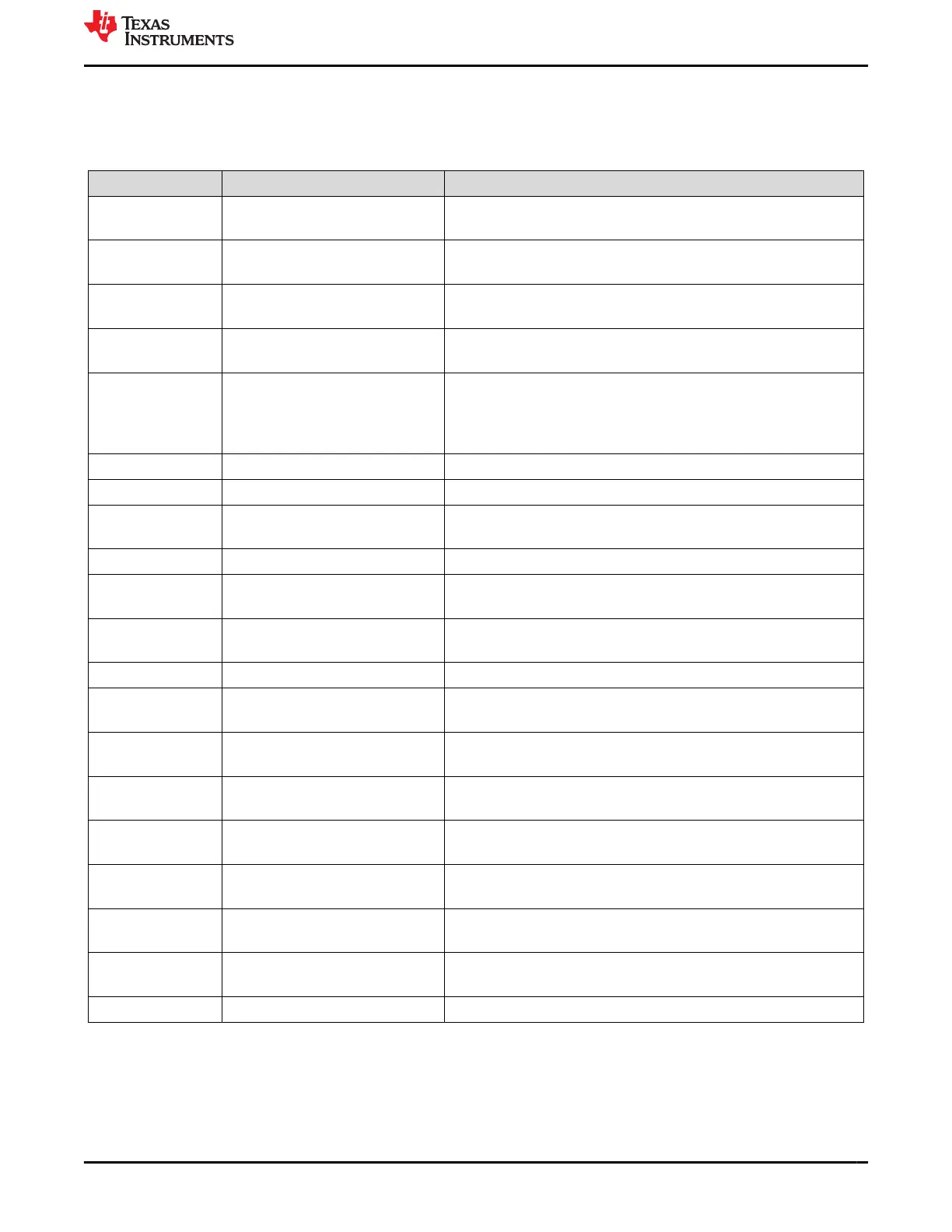
Table 3-1. EVM Board Connections
Test Point Connection Description
TP1, J1 OUTA Connected to the gate driver in the design. Components R5, C5 can be
used to test different R/C loads.
TP2, J2 OUTB Connected to the gate driver in the design. Components R6, C6 can be
used to test different R/C loads.
TP3, J3 SRA Connected to the gate driver in the design. Components R7, C7 can be
used to test different R/C loads.
TP4, J4 SRB Connected to the gate driver in the design. Components R8, C8 can be
used to test different R/C loads.
TP5, TP6 CS_LIM Input for current sense in the design. The CS_LIM circuit provides small
triangle waveform from OUTA, OUTB. Note that this can load OUTA,
OUTB causing a slow in the slew rate. If R9 and R10 are unpopulated,
CS_LIM can be force from TP5.
TP7 VIN Voltage input for the TPS7H5001-SP device
TP8 EN Enable pin for the TPS7H5001-SP device, currently pulled high to VLDO
TP9 COMP Error amplifier output for the TPS7H5001-SP, forcing this voltage runs the
TPS7H5001-SP in open loop.
TP10 REFCAP Internal reference for TPS7H5001-SP
TP11, TP12 SS In a closed loop design, this slowly increases converter output voltage
during start-up
TP13, TP15 SYNC Inputting a clock on this pin synchronizes the TPS7H5001-SP to a
frequency half of the input frequency
TP14 VLDO Internal voltage rail for device logic
TP20 VSENSE Voltage sense for the TPS7H5001-SP. Connected to converter output
voltage in the full design.
TP21 RSC Slope compensation selection resistor. Sets slope compensation slew rate
internal to the device.
TP22 HICC Configurability for the hiccup time of the converter. While grounded
through a resistor on the EVM, in a full design it is generally a capacitor.
TP23 FAULT A signal high on this node turns the TPS7H5001-SP off for any fault
condition needed
TP24 SP Configurability for the delay between the synchronous rectifiers and main
output
TP25 RT Frequency select for the TPS7H5001-SP. Change this to vary the
frequency of the converter.
TP26 PS Configurability for the delay between the main output and synchronous
rectifiers
TP27 LEB Configurability for the leading edge blanking time of the converter
www.ti.com EVM Connectors and Test Points
SLVUBZ8 – JULY 2021
Submit Document Feedback
TPS7H5001-SP Evaluation Module 5
Copyright © 2021 Texas Instruments Incorporated

 Loading...


