18 www.xilinx.com SP605 Hardware User Guide
UG526 (v1.1.1) February 1, 2010
Chapter 1: SP605 Evaluation Board
4. Linear BPI Flash
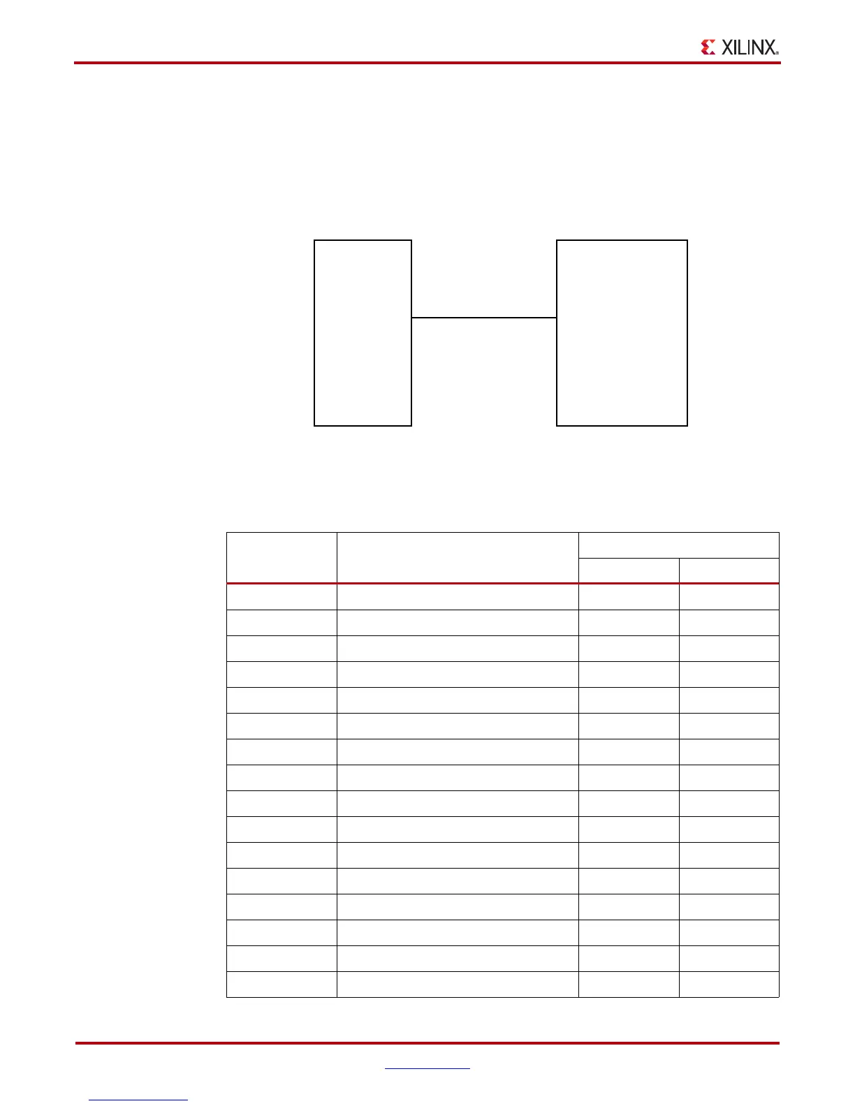
A Numonyx JS28F256P30 Linear Flash memory (U25) on the SP605 (Figure 1-5) provides
32 MB of non-volatile storage that can be used for configuration as well as software
storage. The Linear Flash is operated in asynchronous mode.
For details on configuring the FPGA, see “Configuration Options.”
X-Ref Target - Figure 1-5
Figure 1-5: Linear BPI Flash Interface
Table 1-7: Linear Flash Connections
U1 FPGA Pin Schematic Net Name
U25 BPI FLASH
Pin Number Pin Name
N22 FLASH_A0 29 A1
N20 FLASH_A1 25 A2
M22 FLASH_A2 24 A3
M21 FLASH_A3 23 A4
L19 FLASH_A4 22 A5
K20 FLASH_A5 21 A6
H22 FLASH_A6 20 A7
H21 FLASH_A7 19 A8
L17 FLASH_A8 8 A9
K17 FLASH_A9 7 A10
G22 FLASH_A10 6 A11
G20 FLASH_A11 5 A12
K18 FLASH_A12 4 A13
K19 FLASH_A13 3 A14
H20 FLASH_A14 2 A15
J19 FLASH_A15 1 A16
U1 U25
FPGA
BPI Flash
Interface
Numonyx Type P30
JS28F256P30
ADDR, DATA, CTRL
UG526_05_092409

 Loading...


