SP605 Hardware User Guide www.xilinx.com 9
UG526 (v1.1.1) February 1, 2010
Overview
• 17. Switches
♦ Power On/Off slide switch
♦ System ACE CF Reset pushbutton
♦ System ACE CF bitstream image select DIP switch
♦ Mode DIP switch
• 18. VITA 57.1 FMC LPC Connector
• Configuration Options
♦ 3. SPI x4 Flash (both onboard and off-board)
♦ 4. Linear BPI Flash
♦ 5. System ACE CF and CompactFlash Connector
♦ 6. USB JTAG
• Power Management
♦ AC Adapter and 12V Input Power Jack/Switch
♦ Onboard Power Regulation
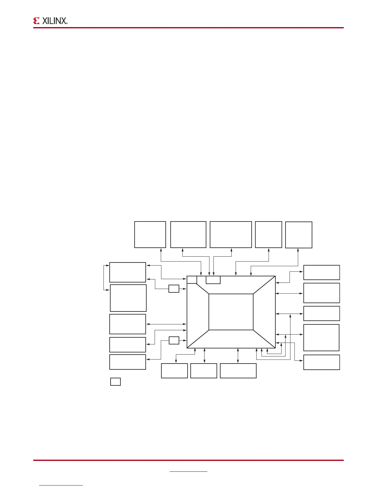
Block Diagram
Figure 1-1 shows a high-level block diagram of the SP605 and its peripherals.
X-Ref Target - Figure 1-1
Figure 1-1: SP605 Features and Banking
Spartan-6
XC6SLX45T-3FGG484
U1
PCIe 125 MHz Clk
SMA REFCLK
SFPCLK
FMC GBTCLK
Bank 0
2.5V
Bank 1
2.5V
Bank 3
1.5V
= Level Shifter
DVI IIC Bus
Bank 2
2.5V
Part of
FMC-LPC
Expansion
Connector
LED
DIP Switch
User SMA x2
1-Lane I/Fs:
PCIe Edge Conn.
SMA x4 SFP
FMC-LPC
10/100/1000
Ethernet PHY,
Status LEDs,
and Connector
SFP IIC Bus
JTAG
System ACE
JTAG
JTAG
MPU I/F
USB JTAG Logic
and USB Mini-B
Connector
DDR3
Component
Memory
Pushbuttons
DIP Switch
LED,
DIP Switch
SPI x4,
SPI Header
Part of FMC-LPC
Expansion Conn.
GPIO Header
USB UART and
USB Mini-B
Connector
DVI Codec and
DVI Connector
Parallel Flash
Main IIC Bus
UG526_01_110409
DED
MGTs
L/S
L/S
L/S

 Loading...


