Getting Started with the VC707 Evaluation Kit www.xilinx.com 11
UG848 (v1.4.1) October 14, 2015
Built-In Self Test
Run BIST
1. Complete the tasks under Preliminary Setup, page 6.
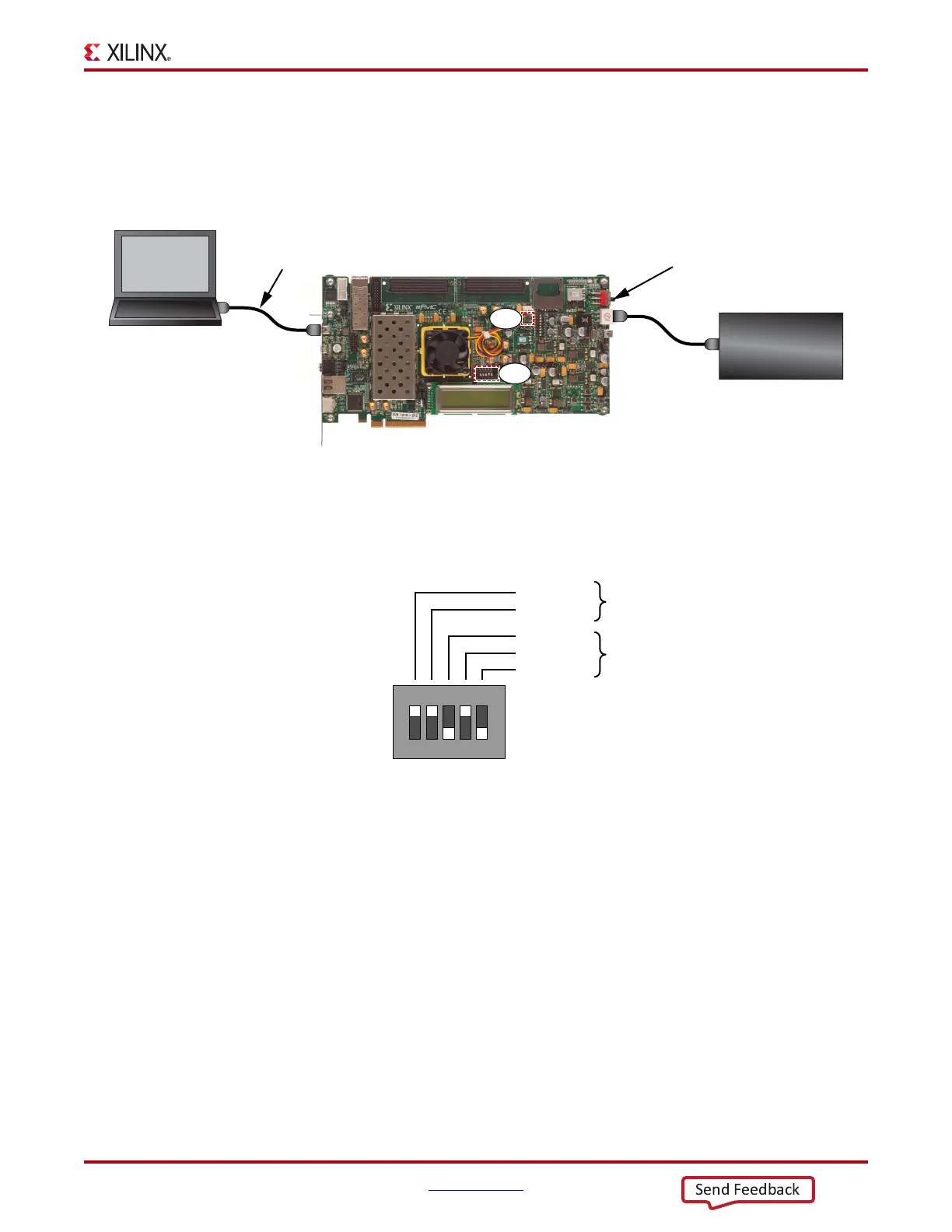
2. Connect the VC707 board to the host computer and power supply as shown in
Figure 1-7.
3. Turn board power on (SW12).
4. Set DIP switch SW11 as shown in Figure 1-8.
X-Ref Target - Figure 1-7
Figure 1-7: BIST Board Connections
UG848_c1_06_040314
Power Supply
100VAC–240VAC Input
12 VDC 5.0A Output
To J18
Board Power
Switch SW12
Host
Computer
USB cable
standard-A plug
to mini-B plug
SW11
To J17
(UART label)
SW9
X-Ref Target - Figure 1-8
Figure 1-8: SW11 BIST Settings
UG848_c1_07_062112
SW11
1 2345
FPGA_M0
0 (Off)
FPGA_M1
FPGA_M2
FLASH_A24
FLASH_A25
1 (On)
Pin 1
Upper Flash ADDR = 0b11
points to the BIST bitstream
in BPI flash memory at U3
Master BPI Mode = 0b010
configures FPGA from
BPI flash memory at U3

 Loading...


