Getting Started with the VC707 Evaluation Kit www.xilinx.com 9
UG848 (v1.4.1) October 14, 2015
Preliminary Setup
Verify Jumpers are in Default Positions
Verify the jumpers on the VC707 board are positioned as shown in Table 1-1. See Figure 1-6
for the location of the jumpers.
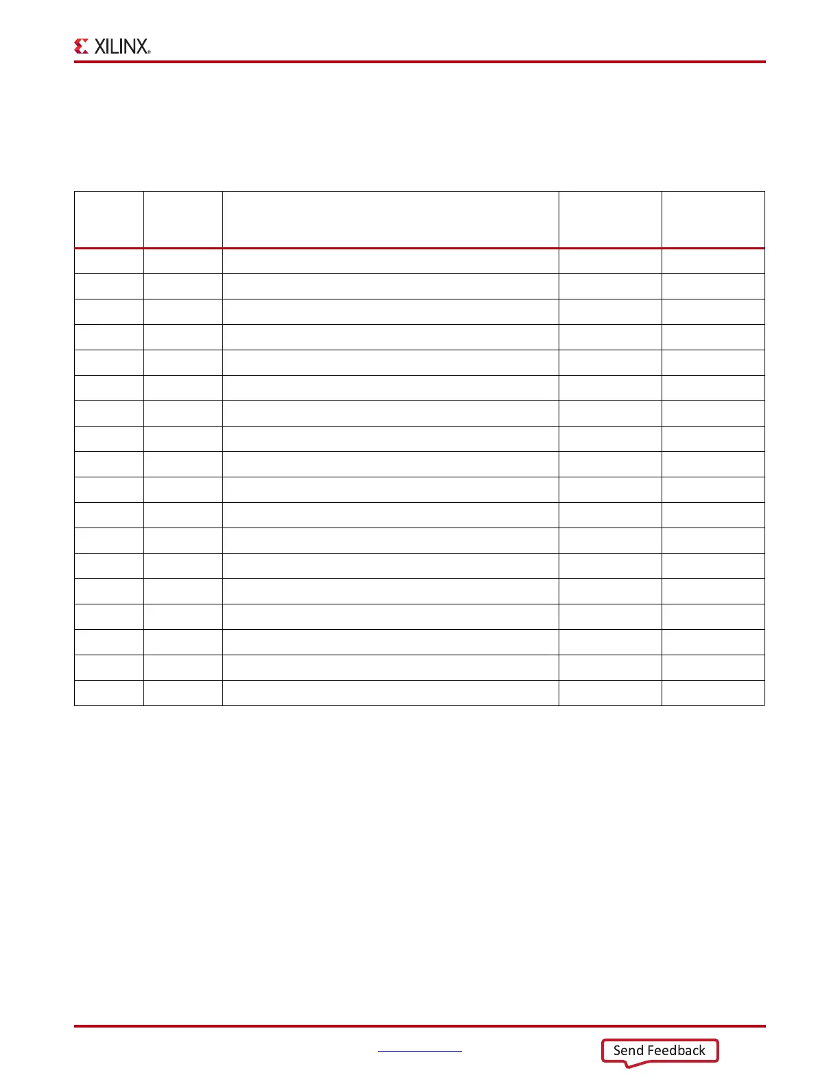
Table 1-1: Default Jumper Settings
Callout Jumper Function
Default Jumper
Position
Schematic
0381418 Page
Number
1 J6 SFP Enable None 31
2 J9 XADC GND ferrite filter bypass jumper None 40
3 J10 XADC GND-to-XADC_AGND jumper 1–2 40
4 J11 TI Controller U42 Addr 52 Reset jumper None 46
5 J12 TI Controller U43 Addr 53 Reset jumper None 50
6 J13 USB Mini-B Connector J2 VBUS None 44
7 J14 USB SMBC U8 CLKOUT selector None 44
8 J38 SFP RX Rate: 1-2 = Full BW Rate, 2-3 = Low BW Rate 1–2 31
9 J39 SFP TX Rate: 1-2 = Full BW Rate, 2-3 = Low BW Rate 1–2 31
10 J42 XADC external 1.2V or internal VREFP selector 1–2 40
11 J43 XADC VCC Select Header 2–3 40
12 J44 USB Mini-B Connector J2 GND jumper None 44
13 J45 USB SMBC U8 VBUS 1–2 44
14 J49 PCIe Bus Width Select Header 1-2 30
15 J50 TI Controller U64 Addr 54 Reset jumper None 53
16 J51 FMC_VADJ_ON_B jumper 1–2 46
17 J53 XADC VCC5V0-to-XADC_VCC5V0 jumper 1–2 40
18 J54 XADC REF3012 U35 V
IN
Select 1–2 40

 Loading...


