5
5
4
4
3
3
2
2
1
1
D D
C C
B B
A A
NV SPEC. Reserve(GPIO6&GPIO25)
Rubband
2019/12/23
Rubband
2020/01/07
NV_NVVDDS_EN
NVVDD_PWRGD
DGPU_PWR_EN
DGPU_RST#_PCH
GPU_PEX_RST#
GPU_PEX_RST#
GPIO25_FBVDD_PSI#
GC6_FB_EN_PCH
NV_EN_DOWN
NV_NVVDD_EN
NV_EN_DOWN
NV_FBVDDQ_EN
GPIO25_FBVDD_PSI#_R
3.3V
1V8_AON
1V8_AON 1V8_AON
3.3VS
1V8_AON
GPU_PEX_RST#10,16
GC6_FB_EN_PCH28,39
NV_PEXVDD_EN 52
NV_FBVDDQ_EN 53
GPIO4_1V8_MAIN_EN 16,18
DGPU_PWR_EN 28,39
NV_NV3V3_EN 55
NV_1V8RUN_EN 51,55
NV_1V8AON_EN 55
NV_EN_DOWN27
GPIO1_GC6_FB_EN16
NV_OVERT#16
1V8_AON_PWRGD55
PLT_RST#24,25
DGPU_RST#_PCH16,28
NV_NVVDD_EN 50,51
GPIO6_NVVDD_PSI#16 GPIO25_FBVDD_PSI#16
FP_FUSE_GPU 19
GPIO26_FP_FUSE16
NVVDD_PWRGD10,50
1V8_AON10,12,13,14,15,16,19,54,55
VDD34,24,25,27,30,32,33,34,36,38,39,40,41,42,43,46,47,49,50,51,52,53,54,55
3.3V2,21,22,33,34,35,37,41,42,44,45,48,51,52,53
3.3VS8,9,16,18,21,22,23,24,25,26,27,28,29,32,33,34,36,37,38,39,41,42,44,46
GPIO6_NVVDD_PSI#_R 50 GPIO25_FBVDD_PSI#_R 53
Title
Size Document Number R ev
Date: Sheet
of
6-71-NP500-D02
D02
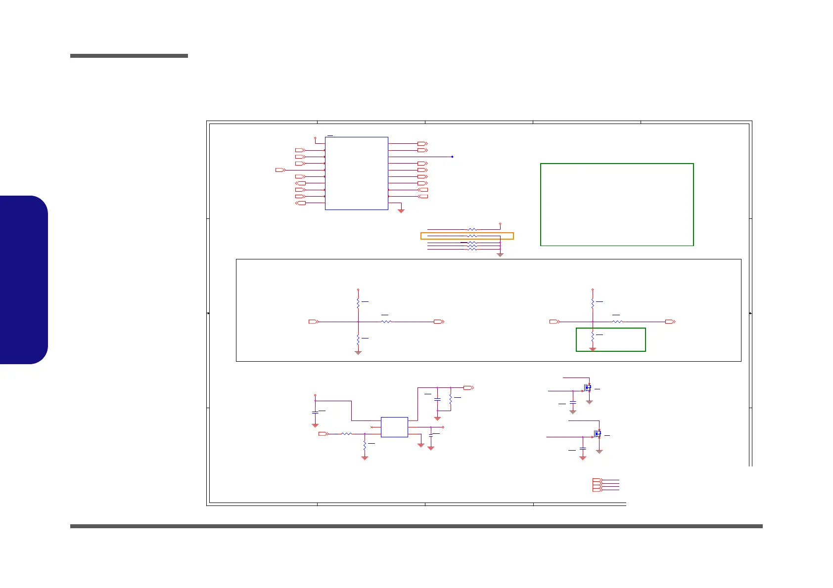
[17] NVIDIA POWER SEQUENCE
A3
17 59Monday, February 24, 2020
ᙔ!Ϻ!ႝ!တ!!DMFWP!DP/
N18P
Title
Size Document Number R ev
Date: Sheet
of
6-71-NP500-D02
D02
[17] NVIDIA POWER SEQUENCE
A3
17 59Monday, February 24, 2020
ᙔ!Ϻ!ႝ!တ!!DMFWP!DP/
N18P
Title
Size Document Number R ev
Date: Sheet
of
6-71-NP500-D02
D02
[17] NVIDIA POWER SEQUENCE
A3
17 59Monday, February 24, 2020
ᙔ!Ϻ!ႝ!တ!!DMFWP!DP/
N18P
R409
*10K_1%_04
NV
R500 10K_04
NV
Q46
*2SK3018S3
NV
G
DS
C621
2.2u_6.3V_X5R_04
NV
R520 10K_04
NV
R372
0_04
NV
R357
2.2K_04
NV
R511 *100K_04
NV
R418
0_04 NV
NV
C645
2.2u_6.3V_X5R_04
NV
U28
SLG4U41681
NV
VDD
1
VIN_DOWN
2
OVERT#
3
SUSB#
4
NVVDDS_PWRGD
5
GC6_FB_EN
6
GC6_FB_EN_PCH
7
PLT_RST#
8
dGPU_RST#_PCH
9
GPU_PEX_RST#
10
FBVDDQ_EN
20
PEX_VDD_EN
19
NVVDDS_EN
18
NVVDD_EN
17
3V3_SYS_EN
16
1V8_MAIN_EN
15
1V8_AON_EN
14
GPIO4_1V8_MAIN_EN
13
dGPU_PWR_EN
12
GND
11
R423
0_04 NV
C641
0.1u_6.3V_X5R_02
NV
R171 *10K_04
NV
R411
10K_1%_04
NV
Q47
*2SK3018S3
NV
G
DS
U18
FA7609A6
P/N = 6-15-76096-7E0
NV
VIN
2
GND
1
NC
3
ON
6
VOUT
4
VBIAS
5
C695
*0.1u_10V_X7R_04
NV
R419
10K_1%_04
NV
R414
10K_1%_04
NV
R495 *10K_04
NV
R371
10K_04
NV
C698
*0.1u_10V_X7R_04
NV
 Loading...