REV.
0
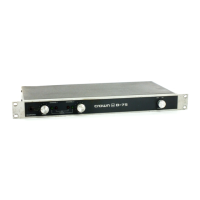
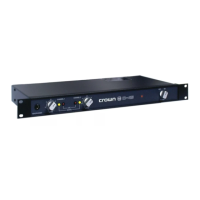
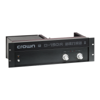
D-75
POWER
AMPLIFIER
6.5.
Final Voltage Amplifier
The
Final
Vo
lta
ge
Amplifier transistor (Q I
02)
is
the
main
voltage amplification stage.
All
signal
vo
ltag
e that
appears
at
the output is developed
here.
R
114
connected
to
the
base circuit
ofQI02
serves
twO
purposes:
I) it provides collector
CUiTent
for
Ql
00
2)
it
provides bias voltage
as
well
as
signal
for
Q 102
As
me
collector current of QlOO varies at
the
frequency
and
amplitude of the incom
in
g signal,
this
same variation
is placed across
the
Final Voltage Amplifier transistor
base
bias
resistor
and
is
impressed
upon
th
base
ofQI02
.
Fig.
6.5 Final
Voltage
Amplifier
6.6. Bias
The output
of
th
e Final
Vo
lta
ge Amplifier provides
the
signal drive to
the
predriver
(Ql
I
0.
Q 107), driver (Q I I
1,
QJ08)
and
output transistors (QI12, QI09)
in
orner
to
amplify
the
current
for
fma
l output power. The correct
bias supply (bias transistor Q103)
voltage of2.IV
DC
is
distributed thro
ug
hout
the
current amplification stages
in
the
following manner:
I) Base
to
Emitter junction
ofQl07
positive predriver
(Q
107)
is
.6V
2)
Base
to
Emitter junction
ofQI08
positive driver
is
.6V
(negative driver Q
III
and outp
ut
transistor QI
12
have
fixed
base emitter bias)
3)
Base
to
Emiuer junction ofQI09, positive output
tra
nsistor
is
.314
V (biased
to
sub
turn-on slate).
As
the
ampli
fier
under loaded operating conditions
increases
in
temperature.
the
bias sensing transistor
(Q
103)
IemperalW'e
inc
reases proportionally. This
condition reduces the
base
to emiucr bi
as
voltage
produced
by
the
bias
supply which results
in
prevention
of
the:mal runaway.
6.
7. Output Stage
There are several categories or classes in ···/hich amplifiers
a.""e
p!a::ed.
<he
mest common being class
A,
B or C.
Each
class or combination thereof,
has
a
sy;':cific
amount
of
bias current
ap
plied to
tilc
transistor which determines its
operating
conditiOl!s.
A class A amplifier,
will
be
biased
such
that a transistor operates always
in
the active region
(360 degrees) between saturation
and cutoff. A class B
amplifier
is
biased at cutoff
(1&0
degrees) and Class C
below cutoff. The
D-75
output stage
is
designed
in
Class
AB+
B
mode
of
o~r.:!tion
where
th
e
d,.-;ver
L."2nsistors
(Q108,
Ql11)
C-.a.T
j
the
bias
CUITen~
whiie the output
transistors (Ql09,
Ql12) serve only
as
boosters. The
output
tran
sis
tors
sense
wilen
the
d.-iver
transistors are
developing significant current
draw
from
the load
and
thus
take over
and
deliver
the
needed
current.
.
",
"
'"
1.!
.~(
j!
".
E.nl
~
~
",
,
".
!t!1
p"'IO!
'Cia
Auf
1
0'09
"
0''''
'K
~
"
!'?
f~
, R,22
•
All
'
,,~
C".
_'"
,.
'.
""
~
_01
0,0/
..
0'>;>
,,,
.
1m
,.
w
.
r~'Ol
,.
,~
~I\l
0'.
0,,,
'fe",
S
'.
f~t
0110
,
,,,
•
I
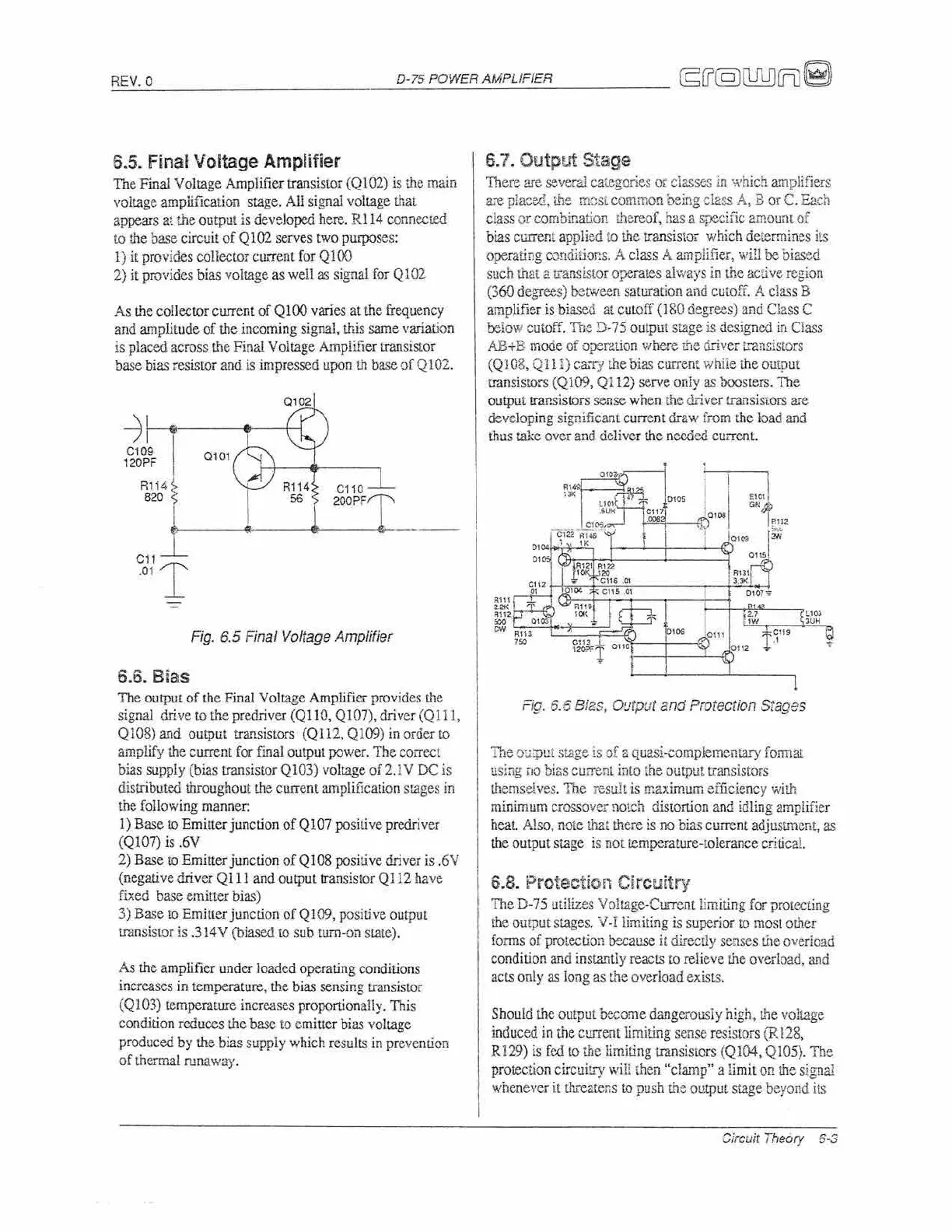
Fig.
6.6 8ies,
O!Jtput
and Protection
Stages
The
O:.ltp
l:t
stage
is
of
a quaskomplemcmary
format
using
ilO
bi(;s
cum;;nt
inlO
the output transistors
themselves.
The result
is
rr:aximum
efGciency
willi
minimum crossover
ooten
dis
tortion
and
idling ampliiier
heat.
A!so,
note tMt there
is
no
bias current adjustmen
t,
as
the output stage
is
nO[
temperature-tolerance critical.
S.8.
Protection Circuitry
The
D-75
utilizes Voltage-Current limiting for protecting
the
omput stages. V
-I
limiting is superior
to
most
other
forms
oi
proteCtion
ty....cause
it directly senses
tile
ove
rl
oad
cond
i
tion
and
instantly reacts
to
rel
ieve
the
overload,
and
acts
only
as
long
as
t.1-te
overioad exists.
Should the
ompul
W..come
dangerousiy high,
the
voh.age
ind
uc
ed
in
the current limiting sense resistors (R
128,
R129)
is
fed
to the limiting transistors
(Q
I04, QJ05). The
protection
circuitry
wi
ll
then "clamp" a limit on
the
signal
whenever it
tr
..
-e<.tens
to
push
the
output stage beyond
its
Circuif Theory 6·3
 Loading...