PCM5100A (DIGITAL : U1052)
Block Diagram
PCM5100, PCM5101, PCM5102
SLAS764 – MAY 2011
www.ti.com
DEVICE INFORMATION
TERMINAL FUNCTIONS, PCM510x
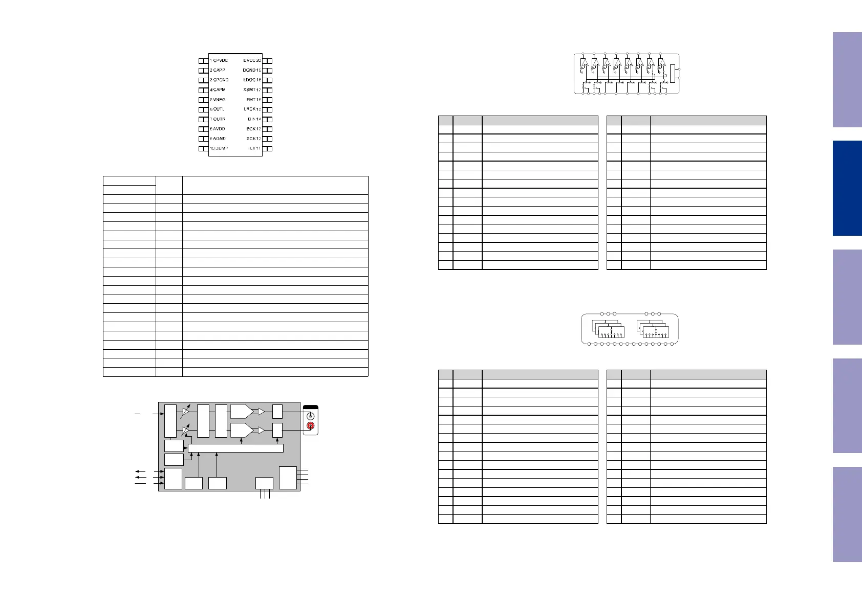
PCM510X (top view)
Table 2. TERMINAL FUNCTIONS, PCM510x
TERMINAL
I/O DESCRIPTION
NAME NO.
CPVDD 1 - Charge pump power supply, 3.3V
CAPP 2 O Charge pump flying capacitor terminal for positive rail
CPGND 3 - Charge pump ground
CAPM 4 O Charge pump flying capacitor terminal for negative rail
VNEG 5 O Negative charge pump rail terminal for decoupling, -3.3V
OUTL 6 O Analog output from DAC left channel
OUTR 7 O Analog output from DAC right channel
AVDD 8 - Analog power supply, 3.3V
AGND 9 - Analog ground
DEMP 10 I De-emphasis control for 44.1kHz sampling rate
(1)
: Off (Low) / On (High)
FLT 11 I Filter select : Normal latency (Low) / Low latency (High)
SCK 12 I System clock input
BCK 13 I Audio data bit clock input
DIN 14 I Audio data input
LRCK 15 I Audio data word clock input
FMT 16 I Audio format selection : I
2
S (Low) / Left justified (High)
XSMT 17 I Soft mute control : Soft mute (Low) / soft un-mute (High)
LDOO 18 - Internal logic supply rail terminal for decoupling
DGND 19 - Digital ground
DVDD 20 - Digital power supply, 3.3V
(1) Failsafe LVCMOS Schmitt trigger input
6
Copyright © 2011, Texas Instruments Incorporated
Audio Interface
8x Interpolation Filter
32bit ∆Σ Modulator
Current
Segment
DAC
Current
Segment
DAC
I/V I/V
Analog
Mute
Analog
Mute
Zero
Data
Detector
UVP/Reset
PLL Clock
Power
Supply
Ch. PumpPOR
Clock Halt
Detection
Advanced Mute Control
MCK
BCK
LRCK
CAPP
CAPM
LINE OUT
DIN (i2s)
PCM510x
CPVDD (3.3V)
AVDD (3.3V)
DVDD (3.3V)
GND
PCM5100, PCM5101, PCM5102
SLAS764 – MAY 2011
www.ti.com
Table 1. Differences Between PCM510x Devices
Part Number Dynamic Range SNR THD
PCM5102 112dB 112dB –93dB
PCM5101 106dB 106dB –92dB
PCM5100 100dB 100dB –90dB
spacer
Figure 1. PCM510x Functional Block Diagram
2 Copyright © 2011, Texas Instruments Incorporated
NJU72343 (INPUT : U4202)
Pin Function
No. Symbol Function No. Symbol Function
1 AREF Analog reference potential terminal 17 DATA IC control data input
2 ADR Address selection terminal 18 CLOCK IC control clock input
3 InA2 Ach input2 19 VDDOUT Digital power supply output terminal
4 InB2 Bch input2 20 AREF Analog reference potential terminal
5 InA1 Ach input1 21 OutH Hch output
6 InB1 Bch input1 22 OutG Gch output
7 InC Cch input 23 OutF Fch output
8 InD Dch input 24 OutE Ech output
9 InE Ech input 25 OutD Dch output
10 InF Fch input 26 OutC Cch output
11 InG1 Gch input1 27 OutB Bch output
12 InH1 Hch input1 28 OutA Ach output
13 InG2 Cch input2 29 AREF Analog reference potential terminal
14 InH2 Dch input2 30 V- negative power supply terminal
15 MUTE External mute control terminal 31 AREF Analog reference potential terminal
16 REF Digital reference potential terminal 32 V+ positive power supply terminal
NJU72750A (INPUT : U4201,U4203)
Pin Function
No. Symbol Function No. Symbol Function
1 V+ positive power supply terminal 17 DATA IC control data input
2 InA1 Ach input1 18 CLOCK IC control clock input
3 InB1 Bch input1 19 NC -
4 InA2 Ach input2 20 NC -
5 InB2 Bch input2 21 OutB3 Bch output3
6 InA3 Ach input3 22 OutA3 Ach output3
7 InB3 Bch input3 23 REF_B Bch reference potential terminal
8 InA4 Ach input4 24 OutB2 Bch output2
9 InB4 Bch input4 25 OutA2 Ach output2
10 InA5 Ach input5 26 REF_A Ach reference potential terminal
11 InB5 Bch input5 27 OutB1 Bch output1
12 InA6 Ach input6 28 OutA1 Ach output1
13 InB6 Bch input6 29 NC -
14 InA7 Ach input7 30 ADR0 Address selection pin 0
15 InB7 Bch input7 31 ADR1 Address selection pin 1
16 REF Reference potential terminal for BIAS 32 V- negative power supply terminal
InA1
OutA
InA2
InB1
InB2
OutB
OutC
InC
OutD
InD
OutE
InE
OutF
InF
InG1
OutG
InG2
InH1
InH2
OutH
Control Logic
InA1
InA2
InA3
InA4
InA5
InA6
InA7
InB1
InB2
InB3
InB4
InB5
InB6
InB7
OutB1
OutB2
OutB3
OutA1
OutA2
OutA3
Before Servicing
This Unit
Electrical Mechanical Repair Information Updating
61
 Loading...