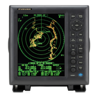
2-22
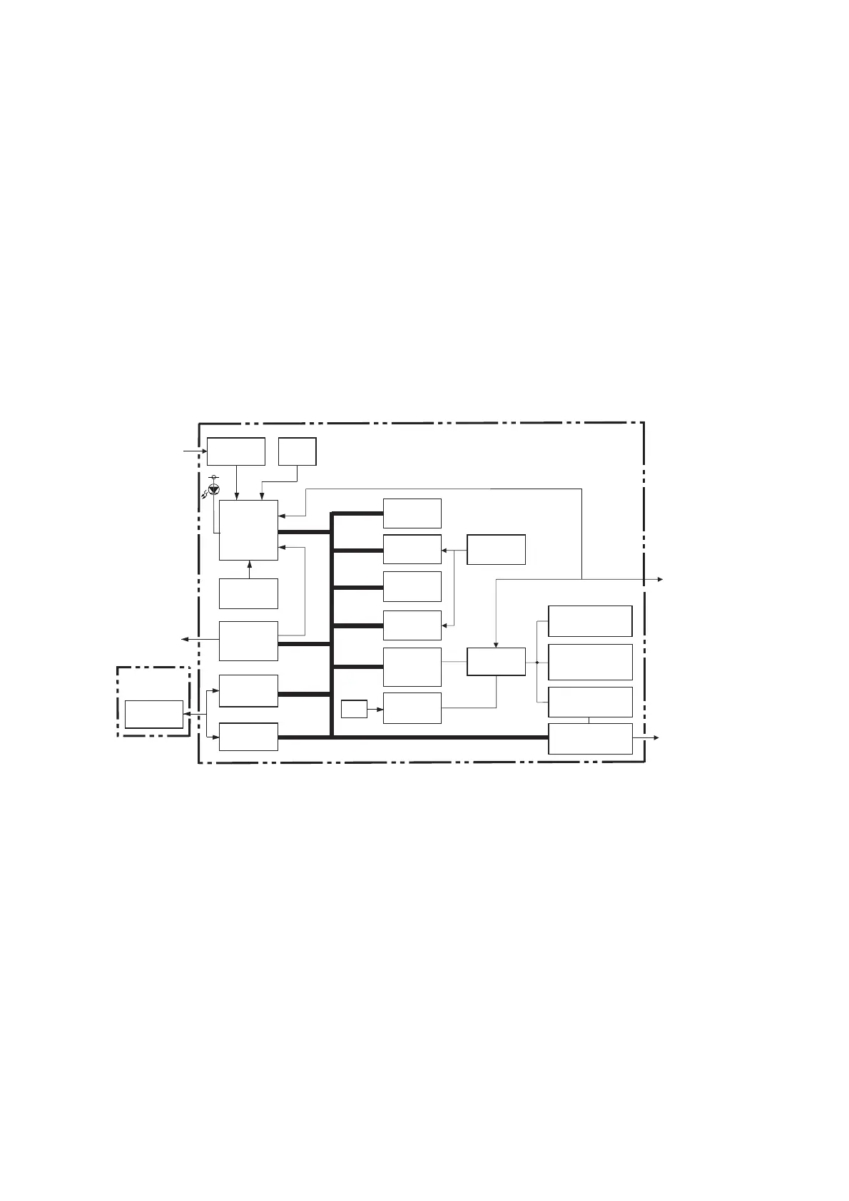
Block Diagram of RP Board
The RP System program is stored on the flash POM, U3 and the program update is performed by
using the program card. The card must be inserted into the upper slot.
The CR1 on the RP board lights when the program is replaced with new one.
RP marks are generated in the following VRAMs or frames on the RP board respectively, and
sent to the SPU board.
1) Track, Mark, and Depth line, etc.;
Uses frames 1 (R:U51), 2 (G:U52) and 3 (B:U53)
2) Grid; uses frames 3 (U53) and 4 (U50)
3) Counter line, and coated land area; uses frame 5 (U49)
Note that waypoint and nav line data is memorized by the SPU board.
Figure 2.13 Block Diagram of RP Board
FR2115-SME-18
Power Fail
U15
DIP SW
P.F
(Activated by H)
CPU (FR-30)
U13
OSC
12.5 MHz
U17
Dual Port RAM
RAM
8 K bytes
U4
Buffer
U22,23,27,
30,31,32
I/O Port
U21
Memory Card
(4 M bytes)
IF Board
14P0299
To SPU Board
(Communication Data)
SRAM
256 K bytes
U8,9
AGDC 2
Controller
U15
DRAM
2 M bytes
U2
Flash Memory
1M bytes U3
Real Time
Clock
U1
Addres & Data
Multiplexer
U28,29
Battery
Back-up
U5
AGDC 2
U14
Addres & Data
Multiplexer
U18,19,20,24,25,26,35
VRAM 4 M bits
(5 frames)
U49
‘
53
Horizontal Scroll
ASIC
U36
Character Gen.
U33
INT 2
(PF)
INT 0
(VSYNC)
Address &
Data Bus
INT 1
(DPRAM)
To SPU Board
(HSYNC, VSYNC,CLK)
To SPU Board
(Video Data)
x4(50 MHz)
OSC
U16
32 MHz
*Working area for running program
*Memory for Track & Mark
*(not used)
CR1
 Loading...