11
22” TFT TV Service Manual
11.9. VPC3230D
11.9.1. General Description
The VPC 323xD is a high-quality, single-chip video front-end, which is targeted for 4:3 and 16:9, 50/60-Hz
and 100/120 Hz TV sets. It can be combined with other members of the DIGIT3000 IC family (such as
DDP 331x) and/or it can be used with 3rd-party products.
The main features of the VPC 323xD are
• high-performance adaptive 4H comb filter Y/C separator with adjustable vertical peaking
• multi-standard colour decoder PAL/NTSC/SECAM including all substandards
• four CVBS, one S-VHS input, one CVBS output
• two RGB/YC
r Cb component inputs, one Fast Blank (FB) input
• integrated high-quality A/D converters and associated clamp and AGC circuits
• multi-standard sync processing
• linear horizontal scaling (0.25 ... 4), as well as non-linear horizontal scaling ‘Panorama-vision’
• PAL+ preprocessing
• line-locked clock, data and sync, or 656-output interface
• peaking, contrast, brightness, color saturation and tint for RGB/ YC
r C b and CVBS/ S-VHS
• high-quality soft mixer controlled by Fast Blank
• PIP processing for four picture sizes (1/4, 1/9, 1/16 or 1/36 of normal size) with 8-bit resolution
• 15 predefined PIP display configurations and expert mode (fully programmable)
• control interface for external field memory
• I
2
C-bus interface
• one 20.25-MHz crystal, few external components
• 80-pin PQFP package
11.9.2. Pin Connections and Short Descriptions
NC = not connected
LV = if not used, leave vacant
X = obligatory; connect as described in circuit diagram
SUPPLYA = 4.75...5.25 V, SUPPLYD = 3.15...3.45 V
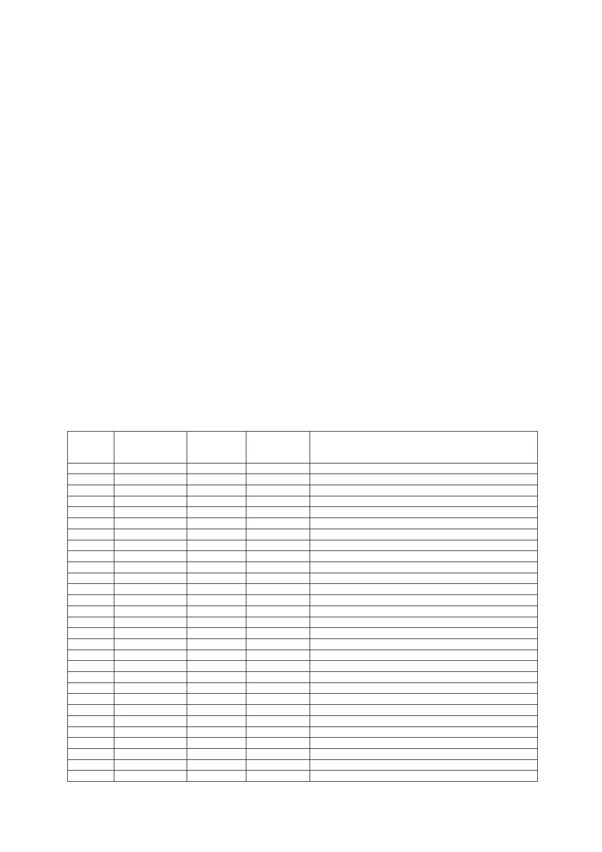
Pin No.
PQFP
80-pin
Pin Name Type Connection
(if not used)
Short Description
1 B1/CB1IN IN VREF Blue1/Cb1 Analog Component Input
2 G1/Y1IN IN VREF Green1/Y1 Analog Component Input
3 R1/CR1IN IN VREF Read1/Cr1 Analog Component Input
4 B2/CB2IN IN VREF Blue2/Cb2 Analog Component Input
5 G2/Y2IN IN VREF Green2/Y2 Analog Component Input
6 R2/CR2IN IN VREF Read2/Cr2 Analog Component Input
7 ASGF X Analog Shield GND
F
8 FFRSTWIN IN LV or GND
D
FIFO Reset Write Input
9 V
SUPCAP
OUT X Digital Decoupling Circuitry Supply Voltage
10 V
SUPD
SUPPLYD X Supply Voltage, Digital Circuitry
11 GND
D
SUPPLYD X Ground, Digital Circuitry
12 GND
CAP
OUT X Digital Decoupling Circuitry GND
13 SCL IN/OUT X I
2
C Bus Clock
14 SDA IN/OUT X I
2
C Bus Data
15 RESQ IN X Reset Input, Active Low
16 TEST IN GND
D
Test Pin, connect to GND
D
17 VGAV IN GND
D
VGAV Input
18 YCOEQ IN GND
D
Y/C Output Enable Input, Active Low
19 FFIE OUT LV FIFO Input Enable
20 FFWE OUT LV FIFO Write Enable
21 FFRSTW OUT LV FIFO Reset Write/Read
22 FFRE OUT LV FIFO Read Enable
23 FFOE OUT LV FIFO Output Enable
24 CLK20 IN/OUT LV Main Clock output 20.25 MHz
25 GND
PA
OUT X Pad Decoupling Circuitry GND
26 V
SUPPA
OUT X Pad Decoupling Circuitry Supply Voltage
27 LLC2 OUT LV Double Clock Output
28 LLC1 IN/OUT LV Clock Output
29 V
SUPLLC
SUPPLYD X Supply Voltage, LLC Circuitry
 Loading...