30
22” TFT TV Service Manual
DS90C365 Pin Description — FPD Link Transmitter
Pin name I/O No. Description
TxIN I 21 TTL level input. This includes: 6 Red, 6 Green, 6 Blue, and 3 control lines —FPLINE,
FPFRAME and DRDY (also referred to as HSYNC, VSYNC, Data Enable).
TxOUT+ O 3 Positive LVDS differentiaI data output.
TxOUT- O 3 Negative LVDS differential data output.
TxCLKIN I 1 TTL Ievel clock input. Pin name TxCLK IN.
R_FB I 1 Programmable strobe select.
TxCLK OUT+ O 1 Positive LVDS differential clock output.
TxCLK OUT- O 1 Negative LVDS differential clock output.
PWR DOWN I 1 TTL level input. Assertion (low input) TRI-STATES the outputs, ensuring low
current at power down.
V
CC
I 3 Power supply pins for TTL inputs.
GND I 4 Ground pins for TTL inputs.
PLL V
CC
I 1 Power supply pin for PLL.
PLL GND I 2 Ground pins for PLL.
LVDS V
CC
I 1 Power supply pin for LVDS outputs.
LVDS GND I 3 Ground pins for LVDS outputs.
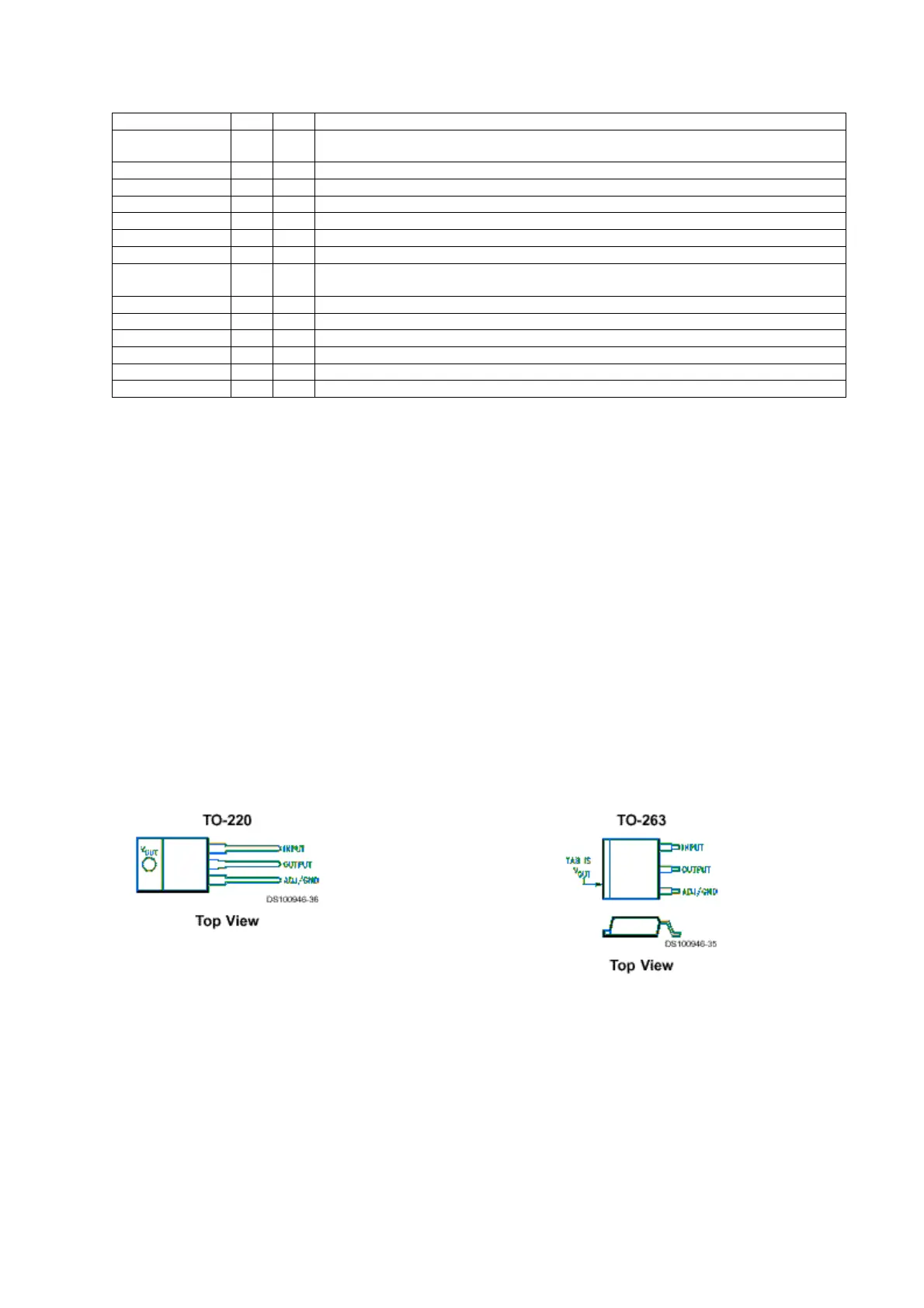
11.22. LM1084
11.22.1. General description
The LM1084 is a series of low dropout voltage positive regulators with a maximum dropout of 1.5V at 5A of
load current. The LM1084 is available in an adjustable version, which can set the output voltage with only
two external resistors. It is also available in three fixed voltages: 3.3V, 5.0V and 12.0V. The fixed versions
intergrate the adjust resistors. The LM1084 circuit includes a zener trimmed bandgap reference, current
limiting and thermal shutdown. The LM1084 series is available in TO-220 and TO-263 pack-ages.
11.22.2. Features
• Available in 3.3V, 5.0V, 12V and Adjustable Versions
• Current Limiting and Thermal Protection
• Output Current 5A
• Industrial Temperature Range -40°C to 125°C
• Line Regulation 0.015% (typical)
• Load Regulation 0.1% (typical)
11.22.3. Connection Diagrams
 Loading...