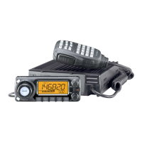
4 - 8
4-4 OTHER CIRCUITS
4-4-1 SUB-CPU RESET CIRCUIT (CONTROL UNIT)
IC2 is the reset voltage detecting circuit. The output voltage
from the +5 regulator circuit (IC5) is applied to the VDD ter-
minal (IC2, pin 2). IC2 outputs “H” (high) signal to the sub-
CPU (IC6, pin 15) when the VDD terminal’s voltage is high-
er than detecting voltage.
IC6 employs the 8-bit CPU.
4-4-2 LCD DISPLAY CIRCUIT (CONTROL UNIT)
The transceiver’s LCD display employs 1/4 duty custom
LCD which displays frequency, S-meter, TX power level, etc.
The LCD display is controlled by the sub-CPU (IC6, pins
41–78) directly.
4-4-3 LCD AND KEY BACK LIGHT CIRCUIT
(CONTROL UNIT)
The sub-CPU (IC6) outputs +8 regulator circuit (Q1, Q3, D5)
control signal from pin 2. The voltage from +8 regulator cir-
cuit is applied to the key back light circuit (DS13–DS18,
DS20, DS23) and LCD back light circuit (DS22).
The back light color is also controlled by the sub-CPU via
the color control circuit (Q6, Q7). The back light has 3 colors
(Umber, Green and Yellow).
Description
The voltage from the external power supply via
the W501 (OPC-465).
The same voltage as the HV line which is con-
trolled by the VCC regulator circuit (Q501). The
circuit is controlled by the power switch controller
(Q502).
Common 8 V converted from the VCC line by the
+8 regulator circuit (IC504).
Transmit 8 V for VHF band which is the same
voltage as the 8V line controlled by the VT8 reg-
ulator circuit (Q19, Q22) using the “VTXC” line.
Transmit 8 V for UHF band which is the same
voltage as the 8V line controlled by the UT8 reg-
ulator circuit (Q20, Q23) using the “UTXC” line.
Common 5 V converted from the HV line by the
+5 regulator circuit (IC503).
Common 5 V converted from the 5V line by the
+5 regulator circuit(Q503, D504). The circuit is
controlled by the power switch controller (Q502).
Common 8 V converted from the 8 V line by the
+8 regulator circuit (Q4).
Common 8 V line which is selected by the
SEL_SW circuit (Q6, Q8). The voltage is applied
to the VHF VCO (VCO board; Q3, D1, D2) and
buffer amplifiers (VCO board; Q4, Q5).
Common 8 V line which is selected by the
SEL_SW circuit (Q6, Q8). The voltage is applied
to the UHF VCO (VCO board; Q101, D100,
D101) and buffer amplifiers (VCO board; Q102,
Q103).
Receive 5 V line converted from the 5VS line by
the R5 regulator circuit (Q24). The circuit is con-
trolled by the “R5CTRL” signal from the CPU
(IC505, pin 78).
Receive 5 V line for AM circuit converted from the
5VS line by the AM5 regulator circuit (Q25). The
circuit is controlled by the “AM” signal from the
CPU (IC505, pin 69).
Receive 5 V line for VHF circuit converted from
the 5VS line by the VHF_R5 regulator circuit
(Q26). The circuit is controlled by the “RXVHF”
signal from the CPU (IC505, pin 73).
Receive 5 V line for UHF circuit converted from
the 5VS line by the UHF_R5 regulator circuit
(Q27). The circuit is controlled by the “RXUHF”
signal from the CPU (IC505, pin 74).
Receive 5 V line for 400 MHz circuit converted
from the 5VS line by the 400_R5 regulator circuit
(Q28). The circuit is controlled by the “RX400”
signal from the CPU (IC505, pin 67).
Receive 5 V line for 800 MHz circuit converted
from the 5VS line by the 800_R5 regulator circuit
(Q29). The circuit is controlled by the “RX800”
signal from the CPU (IC505, pin 66).
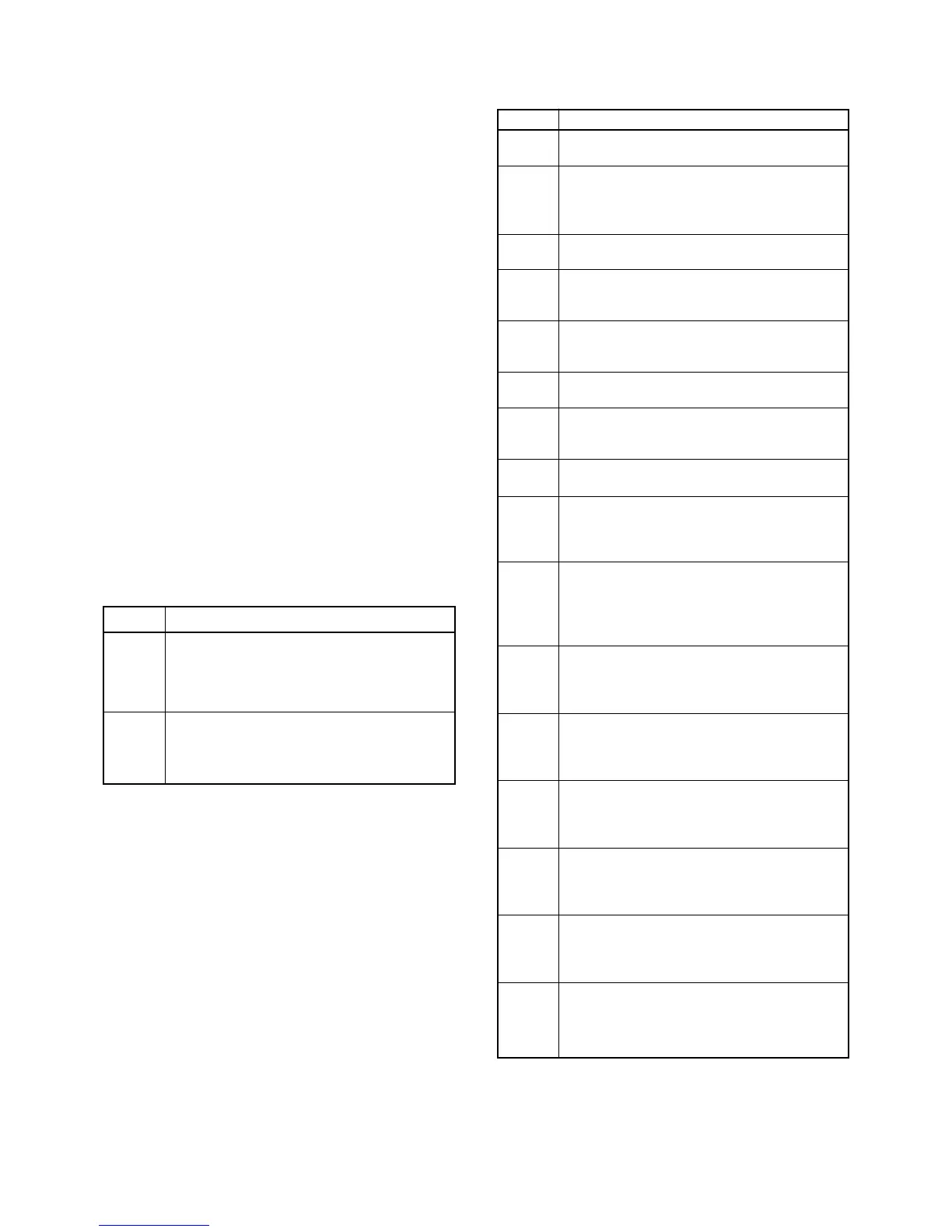
Line
HV
VCC
8V
VT8
UT8
5V
5VS
VCO8
V_VCO8
U_VCO8
R5
AM5
VHF_R5
UHF_R5
400_R5
800_R5
4-5-2 MAIN UNIT VOLTAGE LINES
Description
Common 8 V converted from the HV line by the
+8 regulator circuit (Q1, Q3, D5). The output volt-
age is applied to the LCD back light (DS22) and
key back light (DS13–DS18, DS20, DS21, DS23)
circuits.
Common 5 V converted from the HV line by the
+5 regulator circuit (IC5, D4). The output voltage
is applied to the reset circuit (IC2) and buffer
amplifier (Q2).
Line
8V
CPU5V
4-5 POWER SUPPLY CIRCUITS
4-5-1 CONTROL UNIT VOLTAGE LINES
 Loading...