• 1ST RX IF CIRCUITS
3 - 2
LPF
BPF
XTAL
BPF
XTAL
BPF
XTAL
SPLIT
L1018
HYBRID
COMBINER
PIN DIODE
PIN DIODE
ATT
IF
AMP
RF
AMP
1st RX LO signals
for sub readout
1st RX LO signals for main readout
(64.485-124.455 MHz)
(64.485-124.455 MHz)
LPF
ATT
IF
AMP
RF
AMP
TX CIRCUITS
15K
Fc=60MHz
From the PREAMP BOARD
L904,905
6K
3K
RF UNIT
MCF-N
BOARD
MCF-M
BOARD
MCF-W
BOARD
Fc=60MHz
Q1201
Q1202
D1201,1203,1204
1st RX IF mixer
<-1st RX IF
<-Main readout path
<-Sub readout path
<-1st RX IF
1st RX IF mixer
Q1203-1206
Q1208
D601
D1551
FI6001
FI5001
FI7001
Q1008
D1001-1003
Q1003-1006
Q1001
Q1002
D3702
D3701
LPF
IF
AMP
Q3601-3603
To the 2nd RX IF
circuits
MAIN UNIT
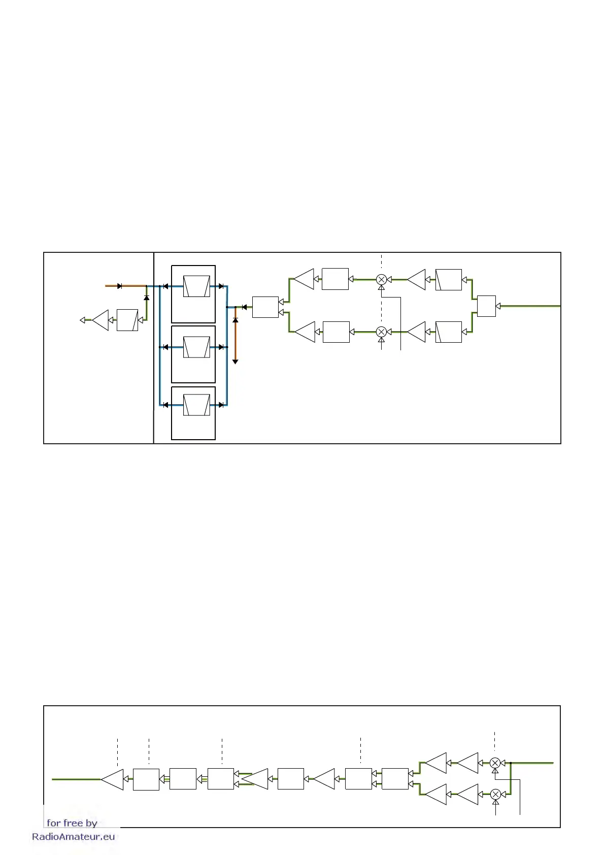
1ST RX IF CIRCUITS (RF UNIT)
The RX signals from the PREAMP BOARD are applied
to the splitter (L904) to divide the received signals for
dualwatch operation.
The separated RX signals are passed through the LPF
which removes unwanted signals (60 MHz and higher), and
amplifi ed by the RF AMP (Main readout; Q1201, 1202/Sub
readout; Q1001, 1002), then applied to the 1st RX IF mixer
(Main readout; Q1203–1206/Sub readout; Q1003–1006).
The RX signals are converted into the 1st RX IF signal by
being mixed with 1st RX LO signals (64.485–124.455 MHz)
from the PLL UNIT.
The converted 1st RX IF signals are passed through the
2-staged attenuator (Main readout; D1201–1203/Sub
readout; D1001–1003) which adjusts the balance of both
1st RX IF signals, and amplified by 1st RX IF AMP (Main
readout; Q1208/Sub readout; Q1008).
These amplified 1st RX IF signals are combined by the
hybrid combiner (L1018), and applied to the 1st IF filter
circuits.
The combined 1st IF signal is passed through one of the
1st IF filters on the MCF-N/-M/-W BOARDS which has
different passband widths. The fi lter to be passed through is
according to the IF fi lter setting.
The fi ltered 1st RX IF signal is applied to the RF UNIT again,
and passed through the LPF and amplified by the RX IF
AMP (MAIN UNIT: 3601–3603).
The amplifi ed 1st RX IF signal is then applied to the 2nd RX
IF circuits.
2ND RX IF CIRCUITS (MAIN UNIT)
The 1st RX IF signal from the 1st RX IF circuits is divided
into two paths, and each signal is applied to the 2nd RX
IF mixers (Image reduction mixer; D3202/D3201) to be
converted into the 2nd RX IF signal, by being mixed with the
2nd RX LO signal (64.494 MHz) from the PLL UNIT.
The image reduction mixer removes image frequency
components by using LO signals which are 90 degrees
phase-shifted from each other.
The converted 2nd RX IF signals are amplifi ed independently
by the buffer (Q3202/Q3201) and IF AMP (IC3203).
These amplifi ed 2nd RX IF signals are 90 degrees phase-
shifted from each other by the phase shifter (IC3202; pins
8-10, pins 12–14). These phase-shifted 2nd RX IF signals
are combined by the combiner (IC3202; pins 5–7) to be
converted into the 3rd RX IF signal.
The converted 3rd RX IF signal is amplified by the 3rd IF
AMP (IC3201), and passed through the limiter (IC3002) and
balance-unbalance converter (Balun; IC4001/IC4002), then
applied to the demodulator circuits.
DEMODULATOR CIRCUITS AND DSP (MAIN UNIT)
The 3rd RX IF signal from the 3rd RX IF circuits is applied
to the A/D converter (IC4004) to be converted into the digital
signal.
The converted digital signal is applied to the DSP (IC5001),
and demodulated and processed.
The demodulated signal is applied to the D/A converter
(IC4301) to be converted into the analog signal, then applied
to the buffer amplifi er (IC4401; pins 1–3).
The buffer amplified AF signals are applied to the RX AF
circuits.
IC4401
To the AF circuits
DSP
I
C5001
D3201
IF
AMP
BALUN
IC4001,
IC4002
BALUN
IF
AMP
IC3203
IC3203
BUFF
Q3202
2nd RX LO signal
D3202
From the 1st
RX IF circuits
IF
AMP
IC3201
BUFF
Q3201
IC3202 IC3202
COMBINER
(64.491 MHz)
LIMITER
IC3002
A/D
IC4004
D/A
I
C4301
90deg.
PHASE
SHIFT
Σ
MAIN UNIT
<-2nd RX IF
<-3rd RX IF<-Digital<-Analog<- RX AF
• 2ND RX IF, 3RD RX IF AND DEMODULATOR CIRCUITS
for
free
by
RadioAmateur.eu
 Loading...