3 - 4
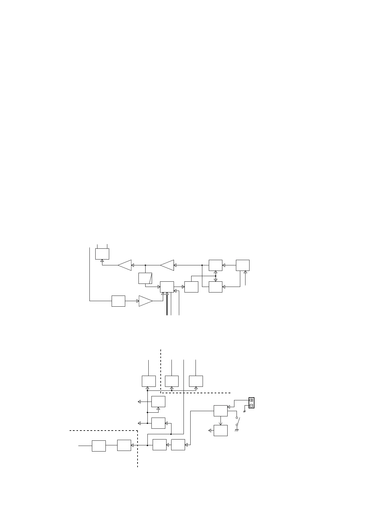
3-3 FREQUENCY SYNTHESIZER CIRCUITS
VCO
A VCO is an oscillator whose oscillating frequency is
determined by the applied volatge. This transceiver has two
VCOs; RX VCO and TX VCO. The RX VCO generates the
1st LO signals for the 1st IF signal produce, and TX VCO
generates TX signal.
The voltage applied to each VCO is passed through the
ripple filter which removes ripples on the VCC line.
• RX VCO
The RX VCO oscillates 79.150 to 98.125 MHz LO signals
for normal RX and WX channels. The generated 1st LO
signals are applied to the 1st mixer (IC68, pin 6) via the
buffer AMPs (Q33, Q35, Q45), TX/RX SW (D36) and the
LPF (harmonic filter).
• TX VCO
The TX VCO oscillates 118.000 to 136.975 MHz transmit
signals. The generated TX signal is applied to the RF
amplifier (Q41) via the buffer AMPs (Q33, Q35), TX/RX SW
(D36).
A portion of the VCO output is applied to the PLL IC via the
buffer and harmonic filter.
PLL (Phase Locked Loop) CIRCUIT
The PLL circuit provides stable oscillation for both of the TX
and 1st LO frequencies (for RX). By comparing feedbacked
VCO output and reference frequency signals, the PLL
corrects the difference of the frequencies.
A portion of RX/TX VCO output is applied to the PLL IC via
buffer (Q33) and harmonic filter. The applied VCO output
is divided according to the serial data including divide ratio
from the CPU, at the prescaler and programmable divider.
In the same way, the reference frequency signal from the
TCXO is applied to the PLL IC and divided so that these
two applied signals are the same frequency.
The divided and frequency-matched signals (VCO output
and the reference frequency signals) are applied to the
phase comparator and phase-compared. The resulted
phase difference is detected as a phase-type signal, and
level-adjusted at the charge pump then output. The output
pulse type signal is passed through the loop filter to be
converted into the DC voltage (=Lock Voltage).
Applying the lock voltage to the variable capacitor which
composes a part of the resonator of RX/TX VCO, the
capasitance of variable capacitor changes corresponding
to the appled lock voltage. This causes the change of
resonation frequency that determine the VCO oscilating
frequency to keep the VCO frequency constant.
When the oscillation frequency drifts, its phase changes
from that of the reference frequency, causing a lock voltage
change to compensate for the drift in the VCO oscillating
frequency.
BUFF BUFF
TX VCO
RX VCO
PLL
IC FILTER
LOOP
FIL
RIPPLE
BUFFTCXO
Q35
Q33
IC47
8
6
2
14
D21
Q5
X2 Q38
Q42
8V
DATA, CLK
UL
LE
2nd LO
Q6, D22
R216–218,
C214,215
LPF
(harmonic
filter)
L51,56,57,
C218,219,225,312
TX/RX
SW
D36
1stLO
TX
• FREQUENCY SYNTHESIZER CIRCUITS
1
2
+5
REG
+8
REG
+3
REG
+5
REG
POWER
SW
LINE
FILTER
8T1 8T2
SW
R8
SW
5V
8V
10C
10C
10C
10 V
REG
Q11
IC31
SW
8T2
8T1
R8
Q32
Q30Q29
MAIN UNIT
PA UNIT
FRONT UNIT
+16
REG
16V
IC75
PWR
SW
IC42
IC44
IC2
IC16
+B
3-4 VOLTAGE DIAGRAMS
Voltage from the power supply is routed to the whole of the transceiver via regulators and switches.
 Loading...