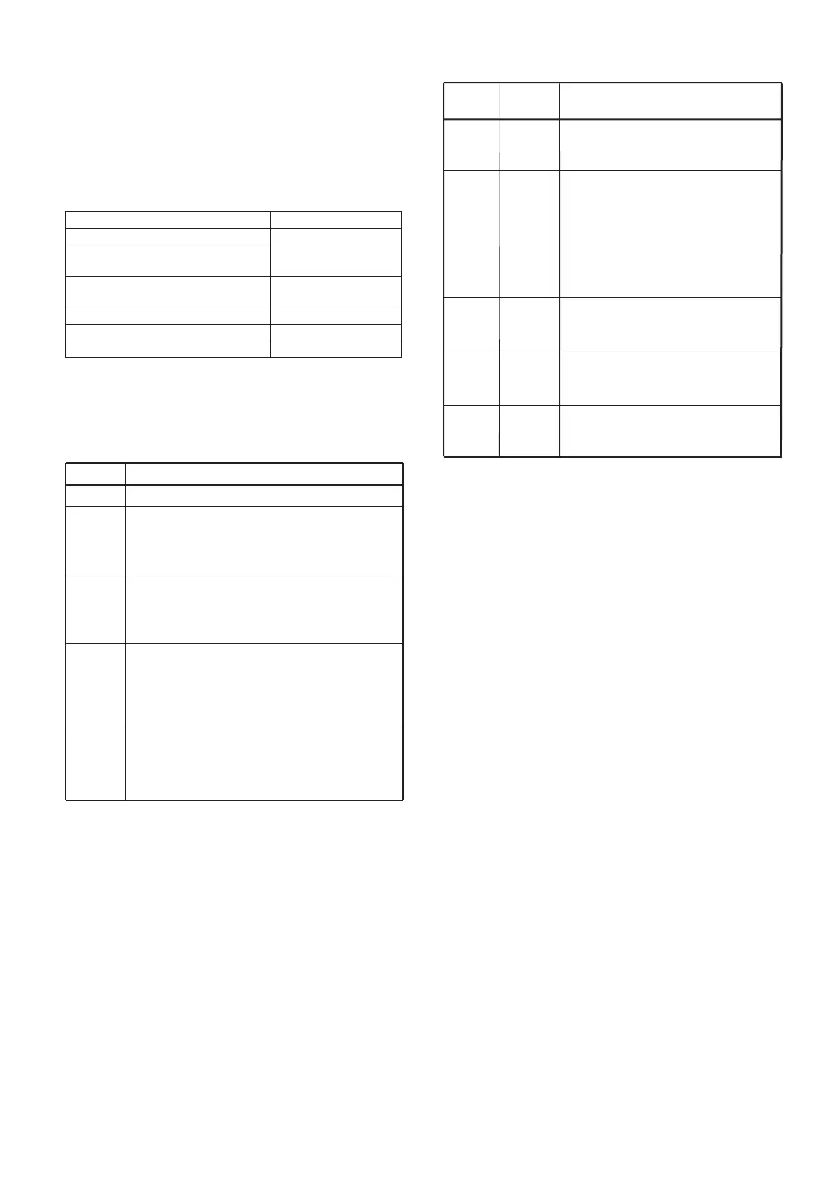
4 - 5
LINE
VCC
+5V
S5V
R5V
T5V
DESCRIPTION
The voltage from the connected battery pack.
Common 5 V converted from the VCC line at
the +5 regulator circuit (IC9). The output voltage
is supplied to the D/A converter (IC8), analog
SW (IC10) and so on.
Common 5 V converted from the VCC line at
the S5 regulator circuit (Q23–Q25). The output
voltage is supplied to the ripple filter (Q17), PLL
IC (IC4), etc.
Receive 5 V converted from the S5V line at the
R5 regulator circuit (Q22). The output voltage
is supplied to the tripler (Q19), FM IF IC (IC1),
IF amplifier (Q4), VCO switch (Q15, Q16), 1st
mixer (Q3), etc.
Transmit 5 V converted from the S5V line at the
T5 regulator circuit (Q21). The output voltage
is supplied to the pre-drive (Q9), APC amplifier
(IC2).
4-5 POWER SUPPLY CIRCUIT
VOLTAGE LINE
4-4 OTHER CIRCUITS
LED CONTROL CIRCUITS
The LED control circuit is composed of the CPU (IC13),
LED driver (Q32) and LED (DS1).
The CPU outputs “RLED” and “TLED” signals from the pins
42 and 43. The signals are applied to the LED driver (Q32,
pins 3 and 1). The driver outputs LED control signals to the
LED (DS1).
BAL
T2
T1
LVA
REF
Outputs the modulation balance level
control signal. The signal is applied to
the buffer amplifier (IC7, pin 3).
•
Outputs the bandpass filter tuning
signal during receive. The output
signal is applied to the bandpass
filters (D9, D10).
• Outputs the TX power control signal
during transmit. The output signal is
applied to the APC amplifier (IC2,
pin 1).
Outputs the bandpass filter tuning
signal. The output signal is applied to
the bandpass filters (D4, D8).
Outputs the PLL lock voltage control
signal. The output signal is applied to
the buffer amplifier (IC7, pin 3).
Outputs the reference oscillator
correcting voltage. The voltage is applied
to the buffer amplifier (IC7, pin 5).
Pin Port
Description
number name
4-6 PORT ALLOCATION
4-6-1 D/A CONVERTER IC (IC8)
11
23
22
14
15
CONDITION COLOR
RECEIVING (2/5-TONE CODE) ORANGE
(Lighting)
LOW BATTERY
(Nearly exhausted)
RED
(Blinks Slowly)
LOW BATTERY
(Almost exhausted)
RED
(Blinks Fast)
CLONING ORANGE
(Blinking)
RECEIVING/SQUELCH OPEN GREEN
(Lighting)
TRANSMITTING RED
(Lighting)
 Loading...