• PLL CIRCUIT
4 - 4
4-3 PLL CIRCUITS
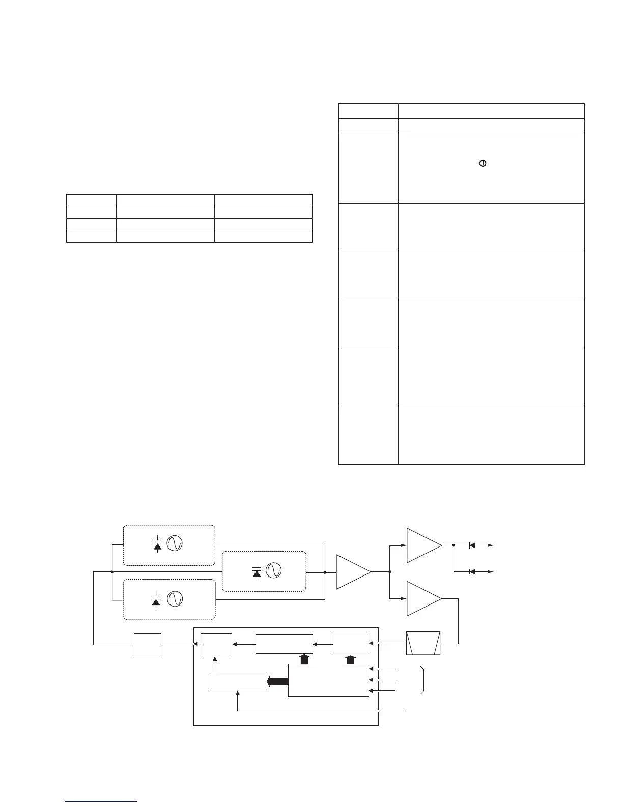
4-3-1 PLL CIRCUIT (MAIN UNIT)
A PLL circuit provides stable oscillation of the transmit fre-
quency and receive 1st LO frequency. The PLL output com-
pares the phase of the divided VCO frequency to the refer-
ence frequency. The PLL output frequency is controlled by
the divided ratio (N-data) of a programmable divider.
The PLL circuit contains the RX VCO1 (Q11, D7, D11), RX
VCO2 (Q12, D9, D13) and TX VCO (Q16, D70, D71). The
oscillated signal is amplified at the buffer amplifier (Q20).
The output signal is applied to the buffer amplifier (Q19),
and is then applied to the PLL IC (IC4, pin 6).
The PLL IC contains a prescaler, programmable counter,
programmable divider and phase detector, etc. The applied
signal is divided at the prescaler and programmable counter
section by the N-data ratio from the main CPU (IC23). The
divided signal is detected on phase at the phase detector
using the reference frequency and output from pin 4. The
output signal is passed through the loop filter (Q46, Q47,
Q50) and is then applied to the VCO circuit.
If the oscillated signal drifts, its phase changes from that of
the reference frequency, causing a lock voltage change to
compensate for the drift in the oscillated frequency.
4-3-2 VCO CIRCUITS (MAIN UNIT)
The VCO circuits contains a separate RX VCO1 (Q11, D9,
D13), RX VCO2 (Q12, D9, D13) and TX VCO (Q16, D70,
D71). The oscillated signal is amplified at the buffer ampli-
fiers (Q20, Q22) and is then applied to the T/R switch (D19,
D20). Then the receive 1st LO (Rx) signal is applied to the
1st mixer (L22, L23, D16) and the transmit (Tx) signal to the
YGR amplifier circuit (Q23).
Loop
filter
PLST
SSO
SCK
4
Q12, D9, D13
RX VCO2
Q11, D7, D11
RX VCO1
TX VCO
Q16 D70, D71
6
10
14
15
16
PLL control signals from CPU (IC23)
15.3 MHz reference signal
from reference frequency osciilator (X2)
IC4 LMX2352TM
Shift register
Prescaler
Phase
detector
Programmable
counter
Programable
divider
Buffer
Q20
Buffer
Q22
Buffer
Q19
to transmitter circuit
to 1st mixer circuit
D19
D20
LPF
4-4 POWER SUPPLY CIRCUITS
Line Description
HV The voltage from a DC power supply.
VCC
The same voltage as the HV line which is
controlled by the power switch circuit (Q41,
Q42). When the [ ] is pushed, the Main
CPU (IC23)outputs the "PWR" control signal
to the power switch circuit to turn the circuit
ON.
CPU 5
Common 5 V converted from the HV line
at the CPU 5 regulator circuit (IC40). The
output voltage is applied to the Main CPU
(IC23) and EEPROM
(IC26), etc.
5V
Common 5 V converted from the CPU 5 line
at the 5 V regulator circuit (Q31, Q32). The
output voltage is applied to the PLL IC (IC4)
and D/A converter IC (IC8), etc.
8V
Common 8 V converted from the VCC line
at the 8 V regulator circuit (IC36). The output
voltage is applied to the buffer amplifi er (Q22)
and AF amplifi er (IC34), etc.
T8V
Transmit 8 V controlled by the T8V regulator
circuit (Q34) using the "TMUT" signal from
the Main CPU (IC23). The output voltage is
applied to the YGR (Q23) and driver (Q48)
amplifi ers, etc.
R8V
Receive 8 V controlled by the R8V regulator
circuit (Q30) using the "TXC" signal from
the Main CPU (IC23). The output voltage is
applied to the RF amplifi er (Q24) and 1st IF
amplifi er (Q6), etc.
• VCO FREQUECY LIST
[L-band] [H-band]
RX VCO1 400.00–434.995 MHz 450.00–484.995 MHz
RX VCO2 435.00–470.00 MHz 485.00–520.00 MHz
TX VCO 400.00–470.00 MHz 450.00–520.00 MHz
A portion of the signal from the buffer amplifier (Q20) is fed
back to the PLL IC (IC4, pin 6) via the buffer amplifier (Q19)
as the comparison signal.
 Loading...