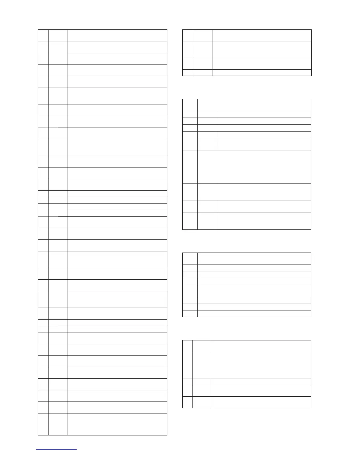
5 - 5
5-5-1 CPU (FRONT UNIT; IC1)
Pin
No.
Port
Name
Description
1−3
KR1−
KR3
Input ports for dealer-programmable keys.
4−8
KS0−
KS4
Output ports for dealer-programmable keys.
10 CCS
Outputs chip-select signal to the attached optional
unit.
19−
21
CENC0−
CENC2
Output ports for CTCSS/DTCS signal.
23 DUSE
Frequency response of tone filter (FRONT UNIT;
IC5) switching signal.
“Low”=While transmitting.
24 IPTT
PTT input from connected microphone.
“Low”=PTT is pushed.
25 HANG
Microphone on/off hook detect.
“Low”=The microphone is off hook.
30 PLST
Outputs PLL strobe signal to the PLL IC (MAIN UNIT;
IC4, pin 11).
34 ULCK
Input port for PLL unlock detect signal from the
PLL IC (MAIN UNIT; IC4, pin 7).
“Low”=While the PLL circuit is unlocked.
39 DSDA
Outputs serial data to the D/A converter (MAIN
UNIT; IC20, pin 6).
43 SENC
Outputs DTMF signals to the LPF (FRONT UNIT;
IC5, pin 3).
44 BEEP
Outputs beep sounds to the LPF (FRONT UNIT;
IC5, pin 7).
45 SDEC Input port for DTMF signals.
46 CDEC Input port for CTCSS/DTCS signals.
48 BATV Input port for power supply voltage.
49 LVIN Input port for VCO lock voltage.
50 RSSI
Input port for receive signal strength level signal
from the IF IC (MAIN UNIT; IC1, pin 12).
51 TEMP
Voltage divided by thermal register (MAIN UNIT;
R209) and R210. (temperature monitor)
52 AFVI
[VOL] dial (FRONT UNIT; R14) input. (divided
voltage of 5V line)
59 RES
Input port for CPU reset signal from the reset IC
(FRONT UNIT; IC8, pin 1).
“Low”=When the CPU is reset.
69 CSFT
Outputs CPU clock shift signal to the clock
frequency shift switch (FRONT UNIT; D6).
71 DAST
Outputs strobe signal to the D/A converter (MAIN
UNIT; IC18, pin 7).
72
IGSW/
DIM
• Ignition SW control input.
Or
• Dimmer control input.
75 NOIS
Input port for noise signal from the IF IC (
MAIN UNIT;
IC1, pin 13).
79 CLO Cloning data output.
80 CLI Cloning data input.
82 ESDA
Outputs serial data to the EEPROM (FRONT UNIT;
IC3, pin 5).
85 ESCL
Outputs clock signal to the EEPROM (FRONT
UNIT; IC3, pin 6).
86 PWON
Transceiver's power control.
“High”=Power ON.
91 LSO
Outputs serial data to the LCD driver (FRONT UNIT;
IC6, pin 48).
92 LSCK
Outputs clock signal to the LCD driver (FRONT UNIT;
IC6, pin 47).
93 LCS
Outputs chip-enable signal to the LCD driver
(FRONT UNIT; IC6, pin 46).
94 LINH
Outputs display inhibit signal to the LCD driver
(FRONT UNIT; IC6, pin 45).
95 LIGT2
Outputs LCD backlight control signal to the
backlight LEDs (FRONT UNIT; DS1–9) driver
(FRONT UNIT; Q5).
“High”=While the backlight is ON.
Pin
No.
Port
Name
Description
98 SCK
Outputs serial clock signal to the PLL IC (IC4, pin
9) and D/A converters (IC17, pin 3/IC18, pin 8/
IC20, pin 7).
99 SO
Outputs serial data to the PLL IC (IC4, pin 9) and D/
A converters (IC17, pin 3/IC18, pin 8/IC20, pin 7).
100 KR0 Input ports for dealer-programmable keys.
5-5-2 EXPANDER (MAIN UNIT; IC17)
Pin
No.
Line
Name
Description
1 EXST Strobe (load enable) input.
2 SO Serial data input.
3 SCK Serial clock input.
4 RXC T8V, R8V lines and RX VCO ON/OFF control.
5 AFON
AF mute SW (Q35) control.
“Low”=Mute
6 NWC
• RX band width switching signal to the 2nd IF
fi lter SW (D56, 57).
“Low”=Narrow mode
• RX band width switching signal to the phase
shifter SW (Q5).
“Low”=Wide mode
7 RMUT
Outputs AF mute signal to the analog switch
(IC3, pins 12, 13).
“Low”=While the squelch is close or transmitting.
12 HORNO
External device control.
“Low”=Pin 6 of OPC-1939 (if connected) is “Low.”
13 TMUT
Outputs transmit mute signal to the transmit
mute switch (Q46).
“High”=Transmitting is muted.
5-5-3 D/A CONVERTER (MAIN UNIT; IC18)
Pin
No.
Description
2, 3 MIC signal level adjustment.
4, 5 RX AF/MIC signal level adjustment.
16, 17 Tone signal level adjustment.
18, 19
Oscillation frequency control voltage to the reference
frequency oscillator (X2).
20, 21 Modulation signal level adjustment.
22, 23 Beep sound loudness adjustment.
24, 25 Squelch threshold level adjustment.
5-5-4 D/A CONVERTER (MAIN UNIT; IC20)
Pin
No.
Line
Name
Description
1T1
• While receiving
Tuning voltage to the tuned BPF (D4, 8).
• While transmitting
TX power level setting signal to the APC AMP
IC2).
2 T2 Tuning voltage to the tuned BPF (D9, 10).
3TLVA
Oscillation frequency correcting voltage to the TX
VCO (Q13, D16, 18, 31, 53).
4RLVA
Oscillation frequency correcting voltage to the RX
VCO (Q14, D33, 34, 52).
5-5 PORT ALLOCATIONS
 Loading...