4 - 3
4-3 PLL CIRCUITS
4-3-1 GENERAL
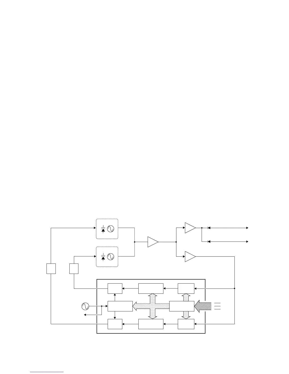
The PLL circuit provides stable oscillation of the transmit fre-
quency and receive 1st LO frequency. The PLL circuit com-
pares the phase of the divided VCO frequency to the refer-
ence frequency. The PLL output frequency is controlled by a
crystal oscillator and the divided ratio of the programmable
divider.
IC2 is a dual PLL IC which controls both VCO circuits for Tx
and Rx, and contains a prescaler, programmable counter,
programmable divider phase detector, charge pomp and etc.
The PLL circuit, using a one chip PLL IC (IC2), directly gen-
erates the transmit frequency and receive 1st IF frequency
with VCOs. The PLL sets the divided ratio based on serial
data from the CPU and compares the phases of VCO sig-
nals with the reference oscillator frequency. The PLL IC
detects the out-of-step phase and output from pins 8 and 13
for Tx and Rx, respectively. The reference frequency (21.25
MHz) is oscillated at X2.
4-3-2 TX LOOP
The generated signal at the TX-VCO (Q7, D6–D8) enters
the PLL IC (IC2, pin 2) and is divided at the programmable
divider section and is then applied to the phase detector
section.
The phase detector compares the input signal with a refer-
ence frequency, and then outputs the out-of-phase signal
(pulse-type signal) from pin 8.
The pulse-type signal is converted into DC voltage (lock
voltage) at the loop filter (R252–R254, C292–C294), and is
then applied to varactor diodes (D6, D7) of the TX-VCO to
stabilize the oscillated frequency.
4-3-3 RX LOOP
The generated signal at the RX-VCO (Q8, D9, D10) enters
the PLL IC (IC2, pin 19) and is divided at the programmable
divider section and is then applied to the phase detector
section.
The phase detector compares the input signal with a refer-
ence frequency, and then outputs the out-of-phase signal
(pulse-type signal) from pin 13.
The pulse-type signal is converted into DC voltage (lock
voltage) at the loop filter (R255–R257, C295, C296), and is
then applied to varactor diodes (D9, D10) of the RX-VCO to
stabilize the oscillated frequency. The lock voltage is also
used for the receiver circuit for the bandpass filter center fre-
quency. The lock voltage from the loop filter is amplified at
the buffer-amplifier (Q6) and then applied to the RF circuit.
4-3-4 VCO CIRCUIT
The VCO outputs from TX-VCO (Q7) and RX-VCO (Q8) are
amplified at the buffer amplifiers (Q9 and Q10), and are then
sent to the Tx/Rx switch (D11, D12). The receive LO signal
is applied to the 1st mixer circuit (Q3) through a low-pass fil-
ter, and the transmit signal is applied to the pre-drive ampli-
fier (Q11). A portion of the VCO output is reapplied to the
PLL IC (IC2, pin 2 or pin 13) via the buffer amplifier (Q5).
 Loading...