5 - 3
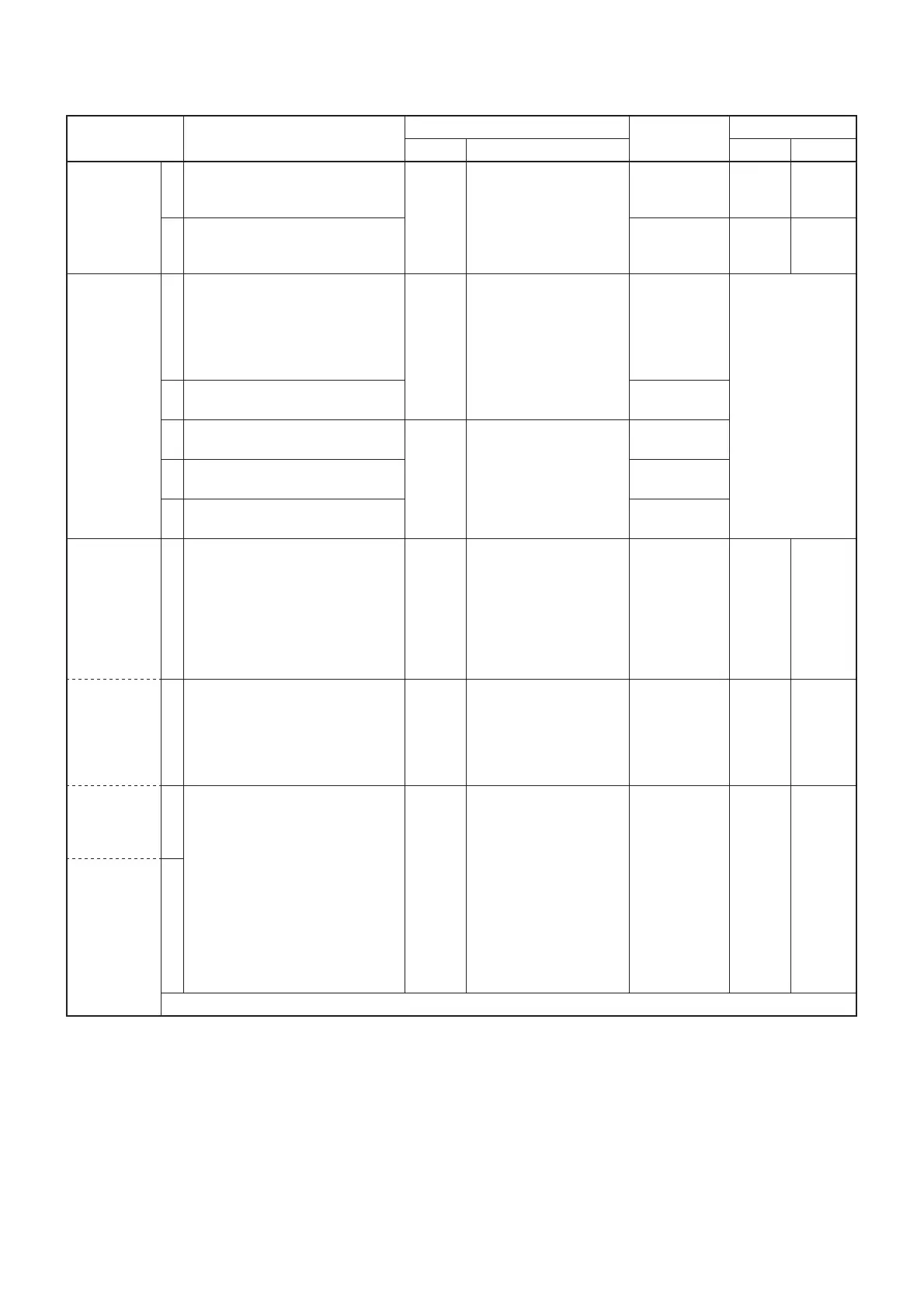
5-2 PLL AND CODEC ADJUSTMENT
ADJUSTMENT ADJUSTMENT CONDITION
MEASUREMENT
VALUE
ADJUSTMENT
UNIT LOCATION UNIT ADJUST
FPGA
FREQUENCY
[ Set FPGA
frequency]
1 • Operating freq. : 1240.00 MHz
• Mode : DD mode
• Receiving
LOGIC-1
unit
Connect a frequency
counter to the check
point "CP200".
16.3840 MHz LOGIC-1
unit
C202
2 • Operating freq. : 1240.00 MHz
• Mode : DV mode
• Receiving
9.8304 MHz LOGIC-1
unit
C215
PLL LOCK
VOLTAGE
1 • Operating freq. : 1240.00 MHz
• Mode : DV mode
• Connect an RF power meter or
50
Ω
dummy load to the antenna
connector.
• Receiving
MAIN
unit
Connect a digital
multimeter or an oscillo-
scope to the check point
"LV1".
More than
0.9 V
Verify
2 • Operating freq. : 1300.00 MHz
• Receiving
Less than
4.4 V
3 • Mode : FM mode
• Receiving
MAIN
unit
Connect a digital
multimeter or an oscillo-
scope to the check point
"LV2".
3.1–4.0 V
4 • Mode : DD mode
• Receiving
2.6–3.3 V
5 • Mode : FM mode
• Transmitting
3.3–4.0 V
I/Q
BALANCE
[ FPGA D.C.
voltage ad-
justment
/DV I]
1• Preset "IQ Direct-current output"
ON.
• Operating freq. : 1270.00 MHz
• Mode : DV mode
• Connect an RF power meter or
50
Ω
dummy load to the antenna
connector.
• Transmitting
MAIN
unit
Connect a digital
multimeter or an oscillo-
scope to the check point
"CP.I".
The same
voltage of the
check point
"CP.IR".
PC
screen
[ FPGA
D.C.
voltage
adjust-
ment
/DV I]
[ FPGA D.C.
voltage ad-
justment
/DV Q]
2 • Transmitting MAIN
unit
Connect a digital
multimeter or an oscillo-
scope to the check point
"CP.Q".
The same
voltage of the
check point
"CP.QR".
PC
screen
[ FPGA
D.C.
voltage
adjust-
ment
/DV Q]
[ FPGA D.C.
voltage ad-
justment
/DV I]
3 • Transmitting Rear
panel
Connect a spectrum
analyzer to the antenna
connector through an
attenuator.
Minimum out-
put level
PC
screen
[ FPGA
D.C.
voltage
adjust-
ment
/DV I],
[ FPGA
D.C.
voltage
adjust-
ment
/DV Q]
[ FPGA D.C.
voltage ad-
justment
/DV Q]
4
•
Repeat step 3 and step 4 several times.
 Loading...