4 - 1
SECTION 4 CIRCUIT DESCRIPTION
4-1 RECEIVER CIRCUITS
4-1-1 ANTENNA SWITCHING CIRCUIT (MAIN UNIT)
The antenna switching circuit functions as a low-pass filter
while receiving and a resonator circuit while transmitting.
This circuit does not allow transmit signals to enter the
receiver circuits.
Received signals from the antenna connector (CHASSIS;
J1) are passed through the low-pass filter which contains
strip-line and C1198, and are then applied to the
λ
⁄4 type
antenna switching circuit (D1160–D1162, L1162).
While receiving, no voltage is applied to D1160–D1162.
Thus, the receive line and ground are disconnected and
received signals are applied to the RF circuit.
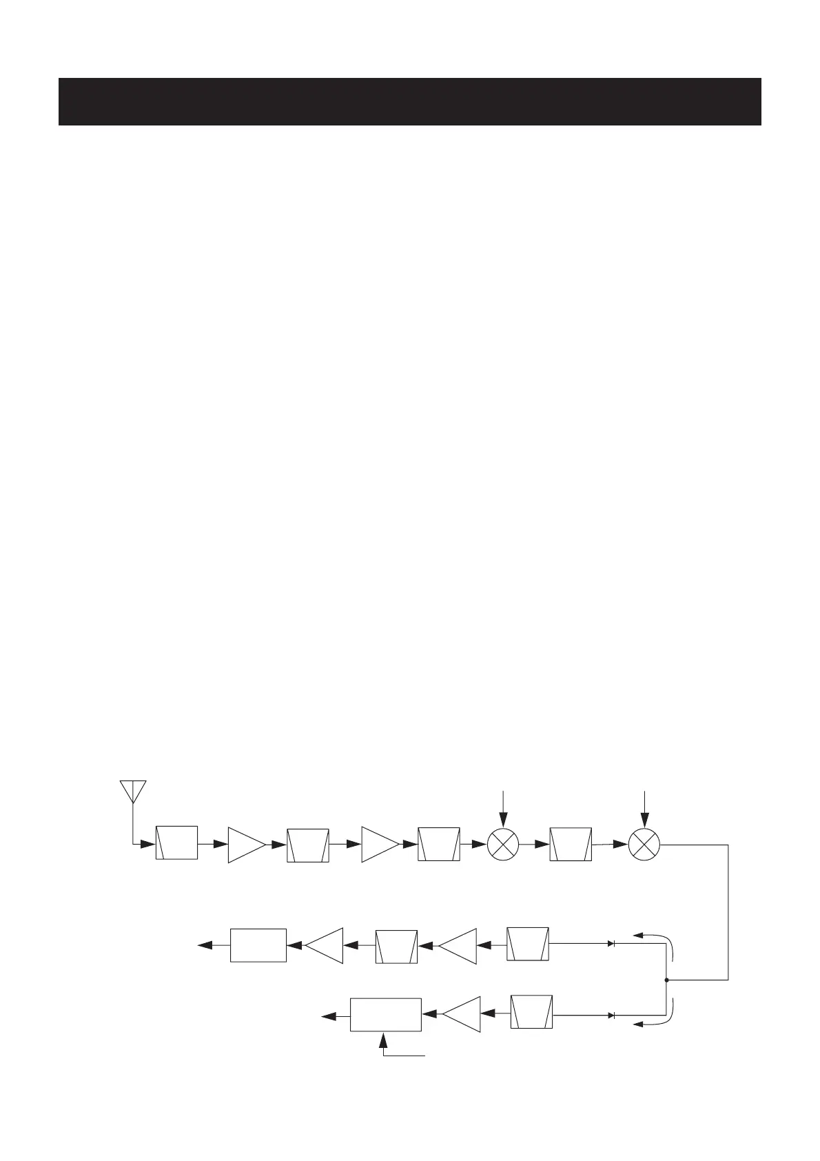
4-1-2 RF CIRCUIT (MAIN UNIT)
The RF circuit amplifies signals within the range of frequen-
cy coverage and filters out-of-band signals.
The signals from the antenna switching circuit pass through
the high-pass filter (L1–L4, C2–C5) and then applied to the
RF amplifier (Q1). The amplifi ed signals are passed through
the bandpass fi lter (FI1) and then applied to the another RF
amplifi er (Q2). The amplifi ed signals are passed through the
another bandpass fi lter (FI2) to suppress unwanted signals.
The fi ltered signal is applied to the 1st mixer circuit.
4-1-3 1ST MIXER AND 1ST IF CIRCUITS (MAIN UNIT)
The 1st mixer circuit converts the received signals into
fixed frequency of the 1st IF signal with the 1st LO signal.
By changing the 1st LO signal, only the desired frequency
passes through the bandpass filter at the next stage of the
1st mixer circuit.
The RF signals from the bandpass filter (FI2) are mixed
with the 1st LO signal, where come from the 1st VCO cir-
cuit, at the 1st mixer circuit (IC71) to produce a 243.95
MHz 1st IF signal. The 1st IF signal is passed through the
bandpass filter (FI71) to suppress unwanted signals and
pass only the desired signals.
The filtered signal is applied to the 2nd IF circuit.
4-1-4 2ND MIXER AND 2ND IF CIRCUITS
(MAIN UNIT)
The 2nd mixer circuit converts the 1st IF signal into the 2nd
IF signal with the 2nd LO signal.
• DV/FM MODE
The filtered 1st IF signal from the bandpass filter (FI71) is
mixed with the 2nd LO signal (275.00 MHz), where come
from 2nd VCO circuit, at the 2nd mixer circuit (Q131) to
produce the 2nd IF signal (31.05 MHz). The 2nd IF signal
is passed through the MCF (FI191) via the DV/FM switch
(D131). The filtered signal is applied to the IF amplifier
(Q191) and then applied to the 3rd mixer circuit in the
demodulator IC (IC191).
• DD MODE
The filtered 1st IF signal from the bandpass filter (FI71) is
mixed with the 2nd LO signal (233.25 MHz), where come
from the 2nd VCO circuit, at the 2nd mixer circuit (Q131)
to produce the 2nd IF signal (10.7 MHz). The 2nd IF signal
is passed through the bandpass filter (FI272) to remove
unwanted heterodyned frequencies via the DD switch
(D273). The filtered signal is amplified at the IF amplifier
(Q270) and then passed through the another bandpass
filter (FI273). The filtered signal is applied to the another IF
amplifier (Q271) and then applied to the MSK receiver IC
(IC271).
FI2
FI1
Q1
Q2
1240–1300 MHz
1st mixer
IC71
1st LO:
3rd LO: 30.6 MHz
AF amplifier
circuit
LOGIC-1 unit
1056.05–1016.05 MHz
2nd IF: 31.05 MHz
2nd IF: 10.7 MHz
Fl71
BPFAMP
AMP
1st IF:
243.95 MHz
2nd mixer
Q131
2nd LO:
DV, FM: 275.00 MHz
DD: 233.25 MHz
HPF
BPF
BPF
FI272
FI273
Q271
Q270
AMP
AMP
BPF
BPF
FI191
D131
D273
DD mode
DV, FM mode
IC191
IC271
Q191
AMP
BPF
Demodulator
IC
MSK
receiver
• RF AND IF CIRCUITS
 Loading...