Datasheet 33
Intel
®
Celeron
®
Processor up to 1.10 GHz
2.11 AGTL+ System Bus Specifications
It is recommended that the AGTL+ bus be routed in a daisy-chain fashion with termination
resistors to V
TT at each end of the signal trace. These termination resistors are placed electrically
between the ends of the signal traces and the V
TT voltage supply and generally are chosen to
approximate the substrate impedance. The valid high and low levels are determined by the input
buffers using a reference voltage called V
REF. Single ended termination may be possible if trace
lengths are tightly controlled, see the Intel
®
440EX AGPset Design Guide (Order Number 290637)
or the Intel
®
Celeron
®
Processor (PPGA) with the Intel
®
440LX AGPset Design Guide (Order
Number 245088) for more information.
Table 8 below lists the nominal specification for the AGTL+ termination voltage (V
TT). The
AGTL+ reference voltage (V
REF) is generated on the processor substrate (S.E.P. Package only) for
the processor core, but should be set to
2
/
3
VTT for other AGTL+ logic using a voltage divider on
the motherboard. It is important that the motherboard impedance be specified and held to:
• ±20% tolerance (S.E.E.P. and PPGA)
• ±15% tolerance (FC-PGA/FC-PGA2)
It is also important that the intrinsic trace capacitance for the AGTL+ signal group traces is known
and well-controlled. For more details on AGTL+, see the Pentium
®
II Processor Developer's
Manual (Order Number 243502) and AP-585, Pentium
®
II Processor AGTL+ Guidelines (Order
Number 243330).
NOTES:
1. Unless otherwise noted, all specifications in this table apply to all Celeron processor frequencies.
2. V
TT must be held to 1.5 V ± 9%; dICC
VTT
/dt is specified in Table 5. It is recommended that VTT be held to
1.5 V ± 3% while the Intel Celeron processor system bus is idle. This is measured at the processor edge
fingers.
3. V
REF is generated on the processor substrate to be
2
/
3
VTT nominally with the S.E.P. package. It must be
created on the motherboard for processors in the PPGA package.
4. V
TT and Vcc
1.5
must be held to 1.5V ±9%. It is required that VTT and Vcc
1.5
be held to 1.5 V ±3% while the
processor system bus is idle (static condition). This is measured at the PGA370 socket pins on the bottom
side of the baseboard.
5. The value of the on-die R
TT
is determined by the resistor value measured by the RTTCTRL signal pin. The
on-die R
TT
tolerance is ±15% based on the RTTCTRL resistor pull-down of ±1%. See Section 7.0 for more
details on the RTTCTRL signal. Refer to the recommendation guidelines for the specific chipset/processor
combination.
6. V
REF is generated on the motherboard and should be 2/3 VTT ±2% nominally. Insure that there is adequate
V
REF decoupling on the motherboard.
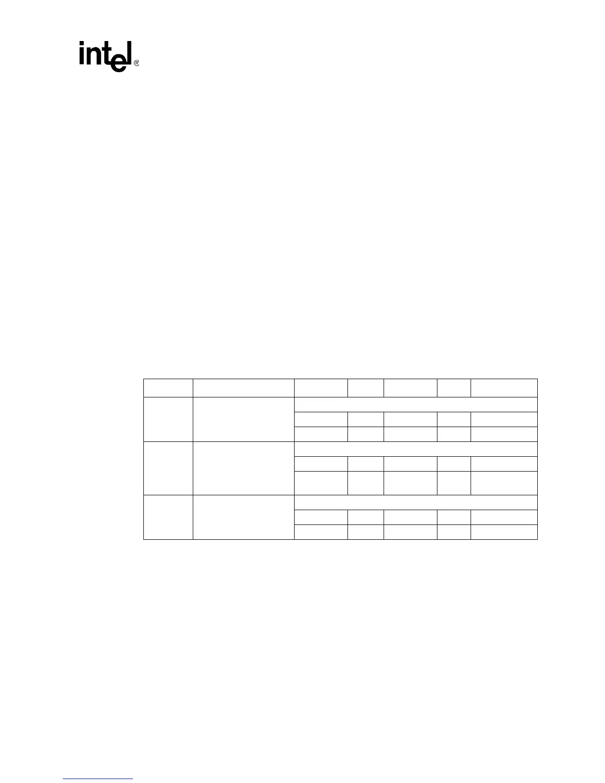
Table 8. Processor AGTL+ Bus Specifications
Symbol Parameter Min Typ Max Units Notes
V
TT
Bus Termination Voltage
• S.E.P.P and PPGA 1.365 1.50 1.635 V 1.5 V ± 9%
2
•FC-PGA/FC-PGA2 1.50 V 4
R
TT
Termination Resistor
• S.E.P.P and PPGA 56 Ω ± 5%
•FC-PGA/FC-PGA2
(on die R
TT)
40 130 Ω 5
V
REF
Bus Reference Voltage
• S.E.P.P and PPGA
2
/
3
VTT V± 2%
3
• FC-PGA/FC-PGA2 0.950 2/3 VTT 1.05 V 6
 Loading...