2-38(No.YA711<Rev.001>)(No.YA711<Rev.001>)2-37
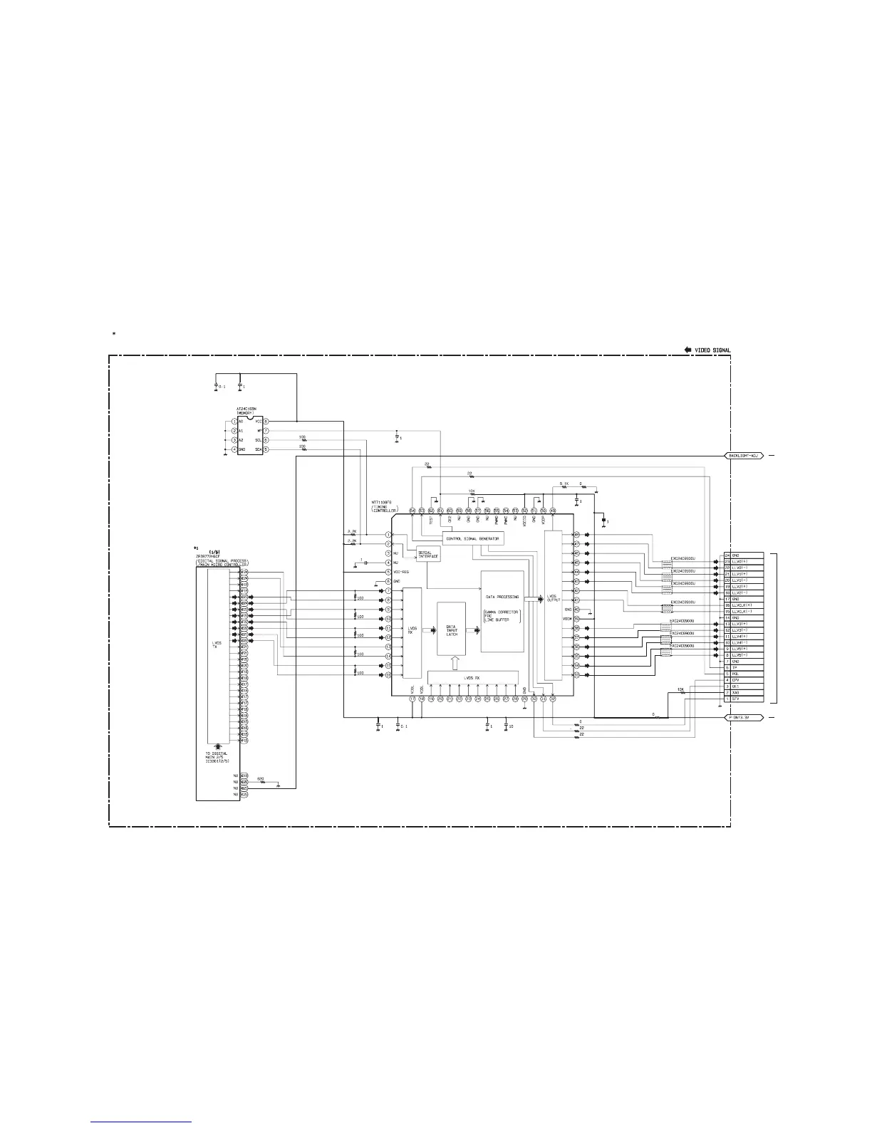
DIGITAL MAIN PWB ASS'Y(1/5)
FU-1ESA19805
A94N5SCD1_0430_1/5_0.0
The order of pins shown in this diagram is different from that of actual IC3301.
IC3301 is divided into five and shown as IC3301 (1/5) ~ IC3301 (5/5) in this Digital Main Schematic Diagram Section.
1 NOTE:
LCD PANEL UNIT
C3901 C3903
R3932
R3909
R3913
R3934
R3916 R3902
C3912
C3911
L3907
CN3902
L3906
L3905
L3904
L3903
L3901
L3902
L3908
R3920
R3917
R3915
R3914
C3902C3910C3927C3924
R3901
R3927
R3928
R3929
R3930
R3931
R3935
IC3901
R3936
C3921
IC3301
C3904
R3933
IC4202
DIGITAL MAIN PWB CIRCUIT DIAGRAM (1/5)
This schematic is only for reference.
Avoid replacing individual parts.
Relpace the entire PWB ASS'Y only.
DIGITAL MAIN PWB(5/5)
DIGITAL MAIN PWB(5/5)
 Loading...