63
(5)
Model Rated Input Voltage
(6)
Model Rated Input Voltage
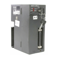
A1SX41 12/24 VDC A1SX71 5/12/24 VDC
A1SX41-S1(S2) 24 VDC
A1SX42 12/24 VDC
A1SX42-S1(S2)
24 VDC
A1SX82-S1*3
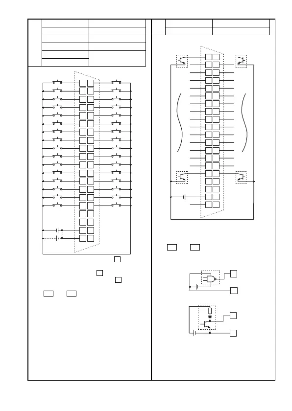
*1 The figure above shows the connections
for the open collector (sink) type.
and are connected internally.
*1
*2
The figure above indicates (the first
half 32 points).
The connections for (the latter half 32
points) are the same as for (regard
X00 to X1F as X20 to X3F.)
and are connected internally.
The A and B pin number rows shown
above are transposed with respect to the
diagram of the A and B rows which is
printed on the module. Remember that
the A row pin numbers correspond to the
B row of the module.
• TTL, LS-TTL, CMOS buffer (sink)
connection
• Sensor (source) connection
*3 A1SX82-S1 can use both positive
common and negative common.
*2 The A and B pin number rows shown
above are transposed with respect to the
diagram of the A and B rows which is
printed on the module. Remember that
the A row pin numbers correspond to the
B row of the module.
Vacant
Vacant
Vacant
Vacant
Vacant
-
+
Vacant
COM
COM
A1
B1
A2B2
A3B3
A4B4
A5
B5
A6B6
A7
B7
A8
B8
A9B9
A10B10
A11B11
A12
B12
A13B13
A14B14
A15B15
A16B16
A17B17
A18B18
A19B19
A20B20
X1F
X1E
X1D
X1C
X1B
X1A
X19
X18
X17
X16
X15
X14
X13
X12
X11
X10
X0F
X0E
X0D
X0C
X0B
X0A
X03
X09
X06
X05
X04
X02
X07
X01
X08
X00
*3
-
+
Vacant
Vacant
Vacant
Vacant
Vacant
-
+
Vacant
COM
COM
A1B1
A2B2
A3B3
A4B4
A5
B5
A6B6
A7
B7
A8B8
A9B9
A10B10
A11B11
A12B12
A13B13
A14B14
A15B15
A16B16
A17B17
A18B18
A19B19
A20B20
X1F
X1E
X1D
X1C
X1B
X1A
X19
X18
X17
X16
X15
X14
X13
X12
X11
X10
X0F
X0E
X0D
X0C
X0B
X0A
X03
X09
X06
X05
X04
X02
X07
X01
X08
X00
B1 B2
F
L
F
B1 B2
B2
-
+
B20
B2
-
+
B20
 Loading...