2-6 THEORY OF OPERATION
4.0 Receiver (for models with PCB 8486473Z04)
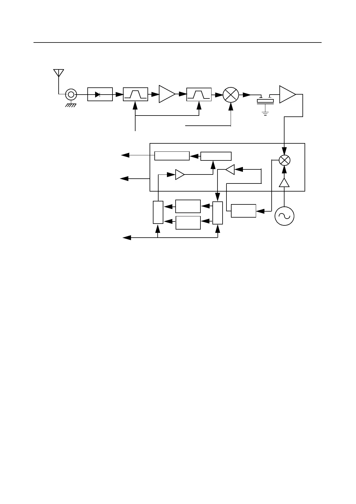
Figure 2-3 VHF Receiver Block Diagram
4.1 Receiver Front-End
(
Refer to Figure 2-3 and the VHF Receiver Front End, VHF Receiver Back End and VHF Transmitter
schematic diagrams
)
The RF signal is received by the antenna and applied to a low-pass filter. For VHF, the filter consists
of L3531, L3532, C3532 to C3563. The filtered RF signal is passed through the antenna switch
consisting of two pin diodes (D3521 and D3551) and a pi network (C3531, L3551 and C3550).The
signal is then applied to a varactor tuned bandpass filter. The VHF bandpass filter comprises of
L3301, L3303, C3301 to C3304 and D3301. The bandpass filter is tuned by applying a control
voltage to the varactor diode (D3301) in the filter.
The bandpass filter is electronically tuned by the DACRx from IC404 which is controlled by the
microprocessor. Depending on the carrier frequency, the DACRx will supply the tuned voltage to the
varactor diodes in the filter. Wideband operation of the filter is achieved by shifting the bandpass
filter across the band.
The output of the bandpass filter is coupled to the RF amplifier transistor Q3302 via C3306. After
being amplified by the RF amplifier, the RF signal is further filtered by a second varactor tuned
bandpass filter, consisting of L3305, L3306, C3311 to C3314 and D3302.
Crystal
Filter
Mixer
Varactor
Tuned Filter
RF Amp
Varactor
Tuned Filter
Pin Diode
Antenna
Switch
RF Jack
Antenna
Control Voltage
from ASFIC
First LO
from VCO
Second LO
IF Amp
455kHz
Filter
Switch
455kHz
Filter
455kHz
Filter
Switch
Demodulator
RSSI
Limiter
Recovered Audio
BW SEL
U3220
 Loading...