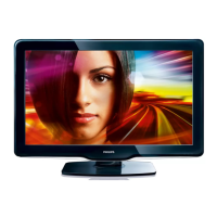
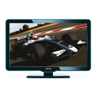
Published by ER/TY 0971 BU TV Consumer Care, the Netherlands Subject to modification EN 3122 785 18542
2009-Nov-20
©
Copyright 2009 Koninklijke Philips Electronics N.V.
All rights reserved. No part of this publication may be reproduced, stored in a
retrieval system or transmitted, in any form or by any means, electronic, mechanical,
photocopying, or otherwise without the prior permission of Philips.
Colour Television Chassis
Q543.1E
LA
18440_000_090205.eps
090226
Contents Page Contents Page
1. Revision List 2
2. Technical Specifications and Connections 2
3. Precautions, Notes, and Abbreviation List 5
4. Mechanical Instructions 9
5. Service Modes, Error Codes, and Fault Finding 14
6. Alignments 33
7. Circuit Descriptions 38
8. IC Data Sheets 47
9. Block Diagrams
Wiring Diagram 32" (P&S) 55
Wiring Diagram 37" (P&S) 56
Wiring Diagram 47" (P&S) 57
Wiring Diagram 52" (P&S) 58
Block Diagram Video 59
Block Diagram Audio 60
Block Diagram Control & Clock Signals 61
Block Diagram I2C 62
Supply Lines Overview 63
10. Circuit Diagrams and PWB Layouts
SSB v1: DC/DC +3V3 +1V2 (B01) 64-65 87
SSB v1: Front End (B02) 66 87
SSB v1: PNX8543 - Power (B03) 67-74 87
SSB v1: Bolt-on (B04) 75-77 87
SSB v1: HDMI (B05) 78-80 87
SSB v1: Class-D (B06) 81 87
SSB v1: Display Interface (Common) (B07) 82-83 87
SSB: SRP List Explanation 84
SSB v1: SRP List Part 1 85 87
SSB v1: SRP List Part 2 86 87
SSB v3: DC/DC +3V3 +1V2 (B01) 88-89 115
SSB v3: Front End (B02) 90 115
SSB v3: PNX8543 - Power (B03) 91-98 115
SSB v3: Bolt-on (B04) 99-101 115
SSB v3: HDMI (B05) 102-104 115
SSB v3: Class-D (B06) 105 115
SSB v3: Display Interface (Common) (B07) 106-107 115
SSB v3: PNX5100 - Power (B08) 108-112 115
SSB v3: SRP List Part 1 113 115
SSB v3: SRP List Part 2 114 115


 Loading...