IC Data Sheets
EN 30 TPM9.2L LA8.
2012-Mar-30
back to
div. table
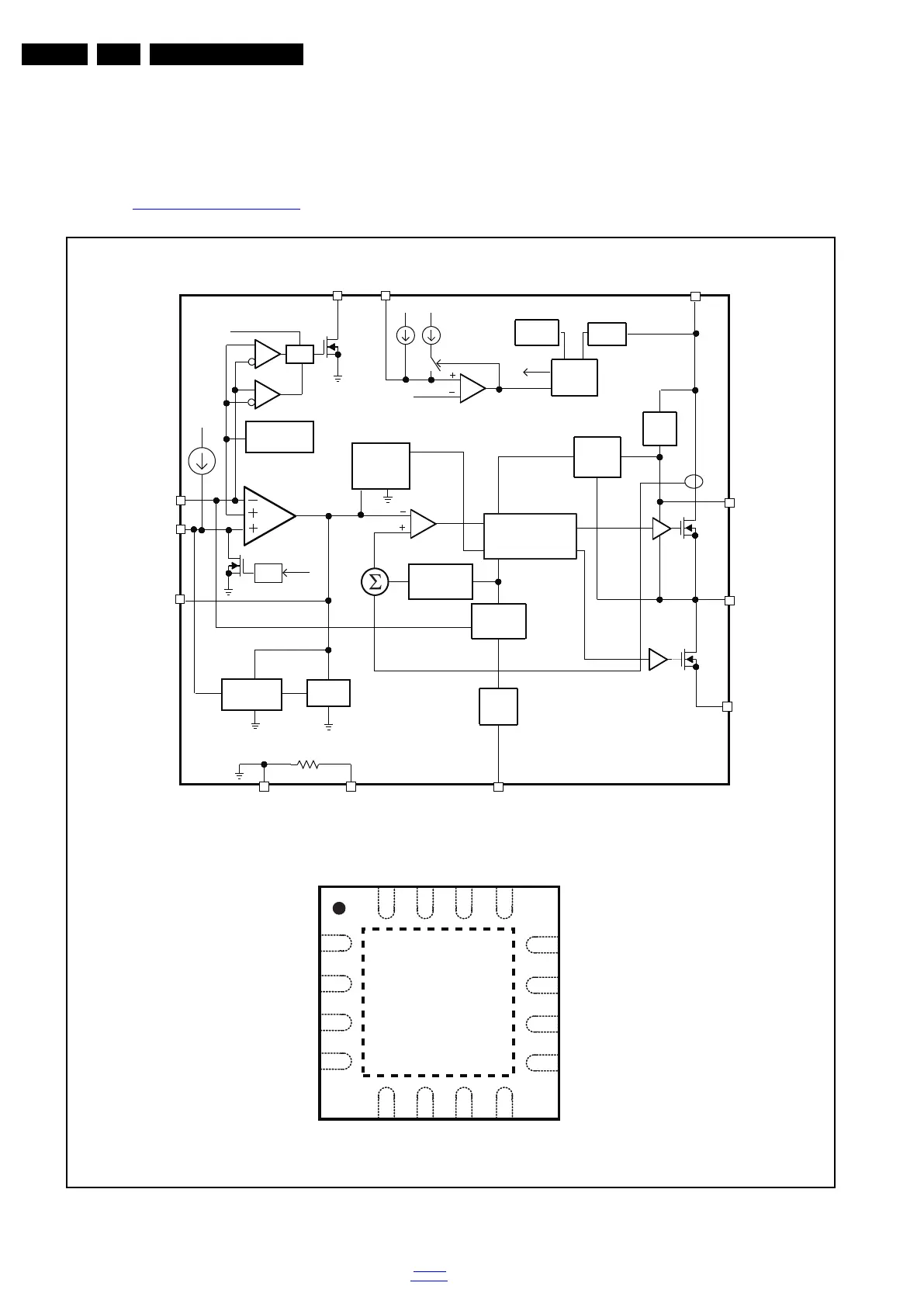
8. IC Data Sheets
This chapter shows the internal block diagrams and pin
configurations of ICs that are drawn as “black boxes” in the
electrical diagrams (with the exception of “memory” and “logic”
ICs).
8.1 Diagram 10-3-1 System Power 1 B12, TPS54319RTER (IC U703)
Figure 8-1 Internal block diagram and pin configuration
19080_310_110408.eps
120102
Block diagram
Pinning information
DGRWP
TOOB
PH
KLC/TR
NE
DNGA
VIN
ESNESV
PMOC
15 14 13
GND
12
11
10
9
8
765
16
GND
VIN
NIV
PH
PH
1
2
3
4
SS/TR
PowerPAD
(17)
QFN16
RTE PACKAGE
(TOP VIEW)
ERROR
AMPLIFIER
Boot
Charge
Boot
UVLO
UVLO
Current
Sense
Oscillator
with PLL
Frequency
Shift
Slope
Compensation
PWM
Comparator
Minimum
COMP Clamp
Maximum
Clamp
Voltage
Reference
Overload
Recovery
VSENSE
SS/TR
COMP
RT/CLK
PH
BOOT
VIN
AGND
Thermal
Shutdown
EN
Enable
Comparator
Shutdown
Logic
Shutdown
Enable
Threshold
Logic
Shutdown
PWRGD
POWERPAD
GND
Logic
S
hutdown
107%
93%
Logic and PWM
Latch
i
1
i
hys
 Loading...