HSPA/UMTS/GSM/GPRS Module Series
UG96&UG95&M95 R2.0 Compatible Design
UG96&UG95&M95 R2.0_Compatible_Design 19 / 42
4 Hardware Reference Design
The following chapters describe compatible design among UG96, UG95 and M95 R2.0 on main functions.
4.1. Power Supply
4.1.1. Power Supply Reference Design
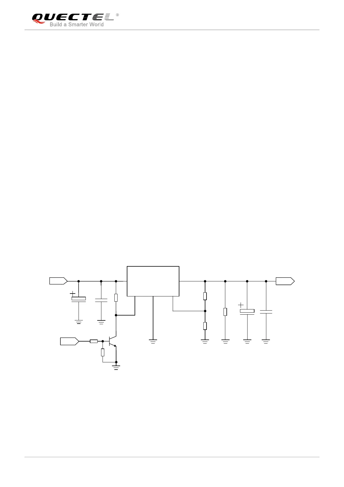
Power design for a module is critical to its performance. The power supply of UG96, UG95 and M95 R2.0
should be able to provide sufficient current up to 2.0A. If the voltage drop between the input and output is
not too high, it is suggested that an LDO should be used to supply power for the module. If there is a big
voltage difference between the input source and the desired output (VBAT), a buck converter is preferred
to be used as the power supply.
The following figure shows a reference design for +5V input power source. The typical output of the power
supply is about 3.8V and the maximum load current is 3.0A.
 Loading...