HSPA/UMTS/GSM/GPRS Module Series
UG96&UG95&M95 R2.0 Compatible Design
UG96&UG95&M95 R2.0_Compatible_Design 20 / 42
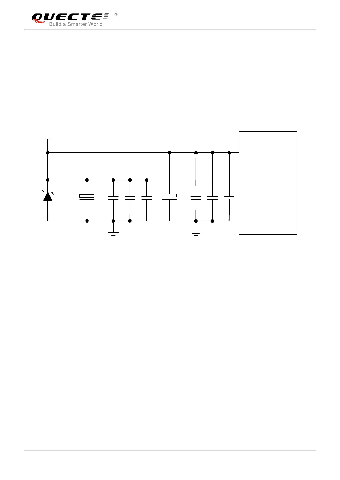
4.1.2. Decrease Voltage Drop
The power supply range of UG96/UG95 is 3.3V~4.3V and the power supply range of M95 R2.0 is
3.3V~4.6V. Please make sure that the input voltage will never drop below 3.3V and exceed 4.3V, and the
typical power supply is 3.8V. The VBAT to UG96/UG95’s VBAT_BB and VBAT_RF pins should be divided
into two separated paths in star structure.
In addition, in order to get a stable power source, it is recommended to use a zener diode with reverse
zener voltage of 5.1V and dissipation power more than 0.5W.
Figure 4: Reference Circuit Design of Star Structure
M95 R2.0 only has two pads for VBAT input, and this is different from UG96/UG95. Therefore, it is not
recommended to mount C1~C4. VBAT_RF pins of UG96/UG95 are compatible with VBAT pins of M95
R2.0.
4.2. Power-on Circuit
UG96/UG95 and M95 R2.0 can be turned on by driving the PWRKEY pin to a low level, though the power
domain of the pin of M95 R2.0 is different from UG96/UG95.
The following circuit is a reference design for turning on the module using PWRKEY.
 Loading...