HSPA/UMTS/GSM/GPRS Module Series
UG96&UG95&M95 R2.0 Compatible Design
UG96&UG95&M95 R2.0_Compatible_Design 26 / 42
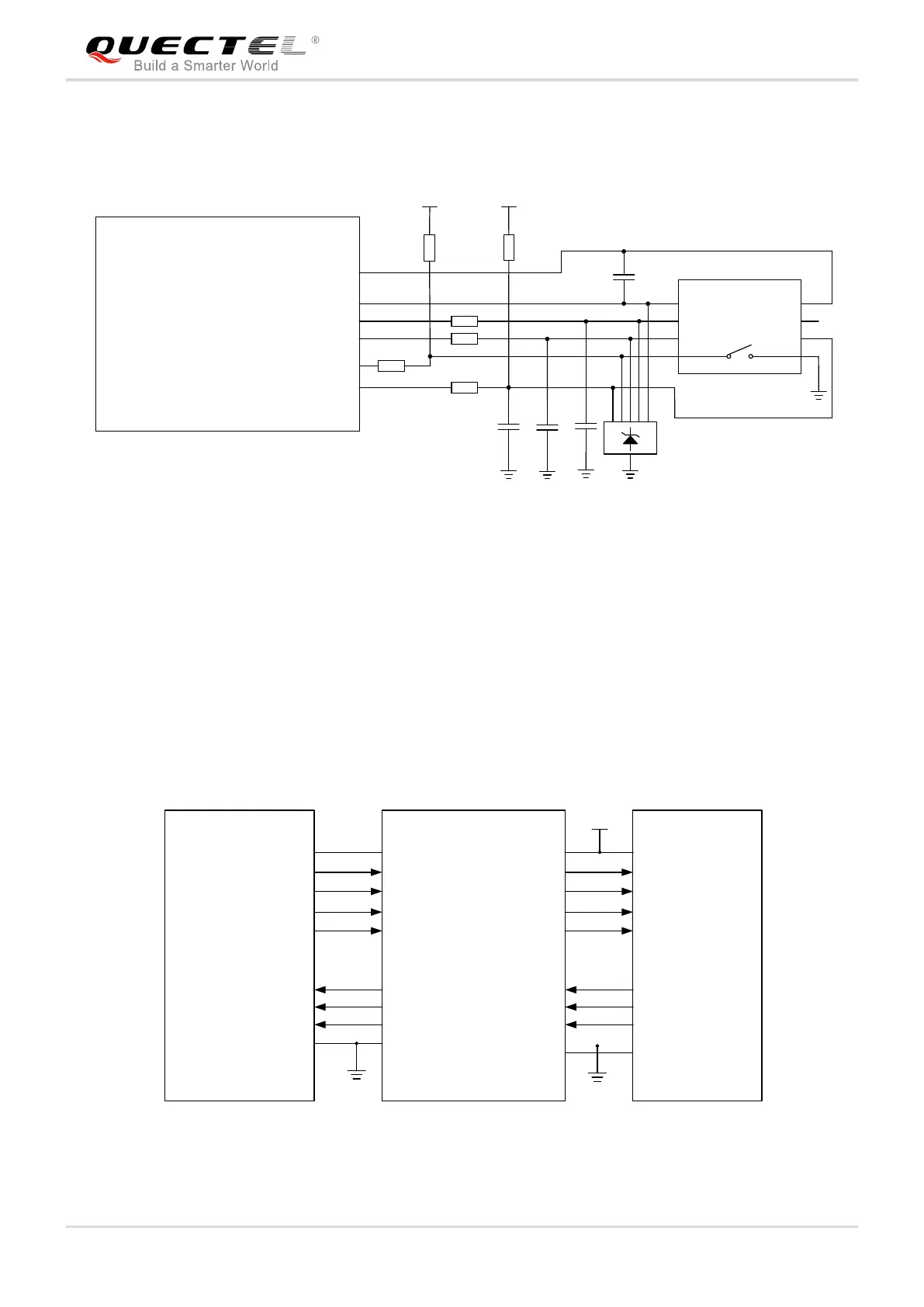
If (U)SIM card detection function is used, keep SIM1_PRESENCE or USIM_PRESENCE pin connected.
A reference design for 8-pin (U)SIM interface is shown in the figure below:
USIM_GND (UG96/UG95)
USIM_PRESENCE (UG96/UG95)
22R
22R
22R
VDD_EXT
51K
100nF
GND
GND
ESD
33pF 33pF 33pF
VCC
RST
CLK
IO
VPP
GND
GND
USIM_VDD (UG96/UG95)
15K
Module
USIM_VDD (UG96/UG95)
USIM_RST (UG96/UG95)
USIM_CLK (UG96/UG95)
USIM_DATA (UG96/UG95)
0R
SIM1_VDD (M95 R2.0)
SIM_GND (M95 R2.0)
SIM1_VDD (M95 R2.0)
SIM1_RST (M95 R2.0)
SIM1_CLK (M95 R2.0)
SIM1_PRESENCE (M95 R2.0)
SIM1_DATA (M95 R2.0)
(U)SIM card connector
Figure 14: Reference Design of 8-Pin (U)SIM Interface
4.7. UART Interface
UG96, UG95 and M95 R2.0 support UART interface. The following circuit shows the reference design for
main UART interface level matching. It is recommended to add a level matching circuit between
UG96/UG95/M95 R2.0 module and MCU due to the different power domain of UART interfaces. For
details, please refer to document [1] & [2].
DCD_M
RTS_M
DTR_M
RXD_M
RI_M
CTS_M
TXD_M
DCD
RTS
DTR
RXD
RI
CTS
TXD
DCD
RTS
DTR
RXD
RI
CTS
TXD
VCCA
GND GND
VDD_EXT VCCB
VCC
DIN1
ROUT3
ROUT2
TXD
DIN4
DIN3
RXD
VCC
MCU
Translator
GND
GND
UG96/UG95/M95 R2.0
Module
Figure 15: Reference Design of Main UART Interface
 Loading...