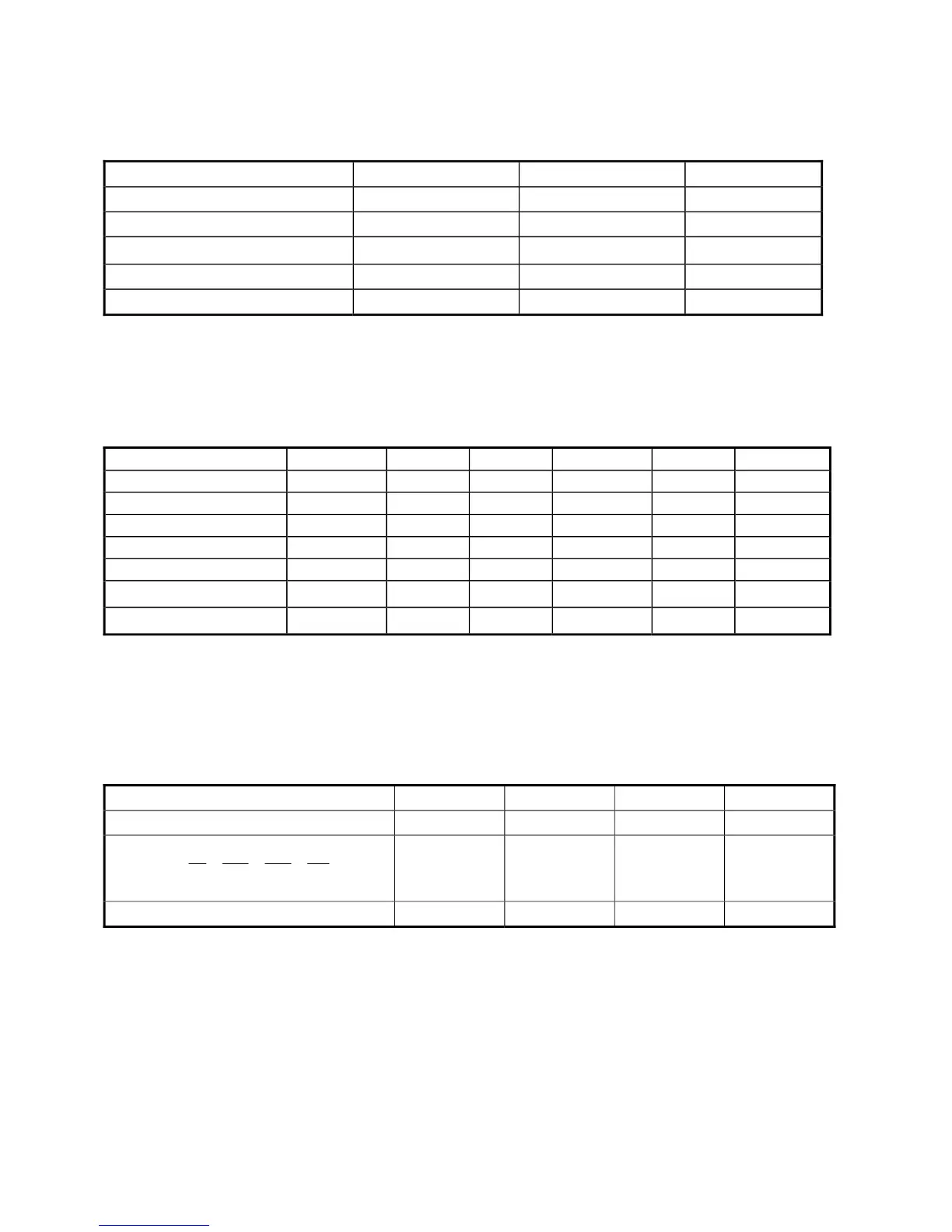
ABSOLUTE MAXIMUM RATINGS
PARAMETER SYMBOL VALUE UNIT
Voltage on any pin relative to VSS VIN, VOUT -1.0 ~ 4.6 V
Voltage on VDD supply relative to VSS VDD, VDDQ -1.0 ~ 4.6 V
Storage temperature TSTG -55 ~ +150
C°
Power dissipation PD 1 W
Short circuit current IOS 50 mA
Note: Permanent device damage may occur if ABSOLUTE MAXIMUM RATING are exceeded.
Functional operation should be restricted to recommended operating condition.
Exposure to higher than recommended voltage for extended periods of time could affect device reliability.
DC OPERATING CONDITION
Recommended operating conditions (Voltage referenced to VSS = 0V, TA = 0 to 70 C° )
PARAMETER SYMBOL MIN TYP MAX UNIT NOTE
Supply voltage VDD, VDDQ 3.0 3.3 3.6 V
Input logic high voltage VIH 2.0 VDD+0.3 V 1
Input logic low voltage VIL -0.3 0 0.8 V 2
Output logic high voltage VOH 2.4 - - V IOH = -2mA
Output logic low voltage VOL - - 0.4 V IOL = 2mA
Input leakage current IIL -5 - 5
μ A
3
Output leakage current IOL -5 - 5
μ A
4
Note: 1. VIH(max) = 4.6V AC for pulse width ≤ 10ns acceptable.
2. V
IL(min) = -1.5V AC for pulse width ≤ 10ns acceptable.
3. Any input 0V ≤ VIN
VDD + 0.3V, all other pins are not under test = 0V.
4. Dout is disabled , 0V ≤ VOUT ≤ VDD.
CAPACITANCE (VDD = 3.3V, TA = 25 C° , f = 1MHZ)
PARAMETER SYMBOL MIN MAX UNIT
Input capacitance (A0 ~ A11, A13 ~ A12) CIN1 2 4 pF
Input capacitance
(CLK, CKE,
CS , RAS , CAS , WE &
L(U)DQM)
C
IN2 2 4 pF
Data input/output capacitance (DQ0 ~ DQ15) COUT 2 5 pF
- 29 -
 Loading...