2929
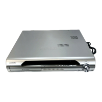
HCD-DX155/DX255
HCD-DX155/DX255
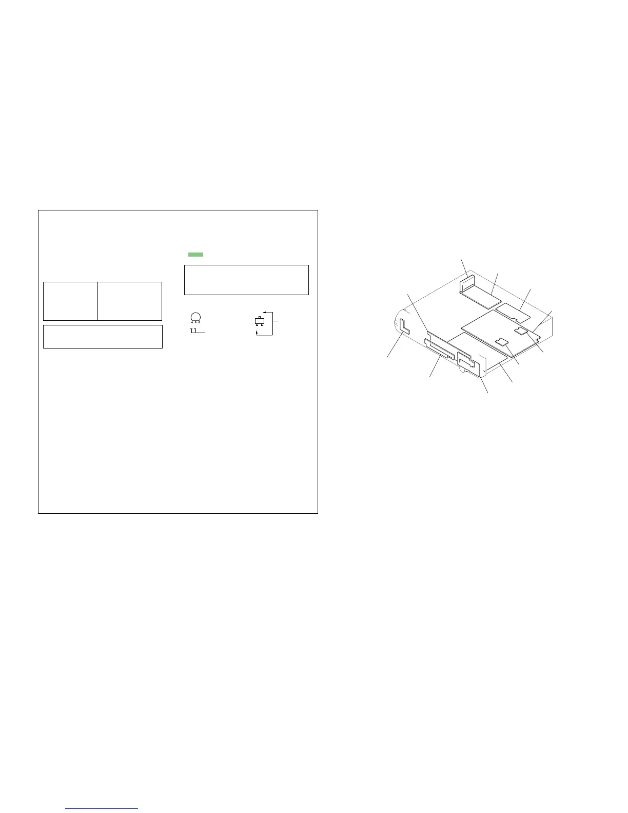
• Circuit Boards Location
SECTION 6
DIAGRAMS
For Schematic Diagrams.
Note:
• All capacitors are in µF unless otherwise noted. (p: pF)
50 WV or less are not indicated except for electrolytics and
tantalums.
• All resistors are in Ω and
1
/
4
W or less unless otherwise
specified.
• f : internal component.
• C : panel designation.
THIS NOTE IS COMMON FOR PRINTED WIRING BOARDS AND SCHEMATIC DIAGRAMS.
(In addition to this, the necessary note is printed in each block.)
• A : B+ Line.
•Voltages and waveforms are dc with respect to ground un-
der no-signal (detuned) conditions.
•Voltages and waveforms are dc with respect to ground in
service mode.
•Waveforms are taken with a oscilloscope.
Voltage variations may be noted due to normal production
tolerances.
no mark : DVD STOP
*
: Impossible to measure
•Voltages are taken with VOM (Input impedance 10 MΩ).
• Circled numbers refer to waveforms.
• Signal path.
F : AUDIO
J : CD PLAY
c : DVD PLAY
I : SACD PLAY
d : TUNER
L : VIDEO
E : Y
a : CHROMA
r : COMPONENT VIDEO
q : R, G, B
f : AUDIO IN
•Abbreviation
AUS: Australian model
CND : Canadian model
E3 : 240V AC area in E model
MX : Mexican model
SP : Singapore model
For Printed Wiring Boards.
Note:
• X : parts extracted from the component side.
• a : Through hole.
• : Pattern from the side which enables seeing.
(The other layers' patterns are not indicated.)
• Indication of transistor.
Caution:
Pattern face side: Parts on the pattern face side seen from
(SIDE A) the pattern face are indicated.
Parts face side: Parts on the parts face side seen from
(SIDE B) the parts face are indicated.
✩ New part of EEP ROM (IC1103) on the MAIN board
cannot be used. Therefore, if the mounted MAIN board
(A-1151-985-A, etc.) is replaced, exchange new EEP
ROM (IC1103) with that used before the replacement.
C
B
These are omitted.
E
Q
CEB
These are omitted
Note:
The components identi-
fied by mark 0 or dot-
ted line with mark 0 are
critical for safety.
Replace only with part
number specified.
Note:
Les composants identifiés
par une marque 0 sont cri-
tiques pour la sécurité.
Ne les remplacer que par une
piéce portant le numéro
spécifié.
FL board
JACK board
LED board
SW board
I/O board
SPEAKER board
MAIN board
HEATSINK (A) board
HEATSINK (B) board
POWER board
TUNER UNIT
 Loading...