EasyManua.ls Logo

Sony HCD-FR1 User Manual

Sony HCD-FR1
138 pages
To Next Page IconTo Next Page
To Previous Page IconTo Previous Page
Page #7 background imageLoading...
Page #7 background image
7
HCD-FR1/FR8/FR9
SECTION 3
DIAGRAMS
• Circuit Boards Location
SPK board
LF board
IO board
FL board
SONY LAMP board
PW KEY board
CONTROL KEY board
DISC KEY board
ROLLER MOTOR board
MODE MOTOR board
SENSOR board
SW (1) board
SW (2) board
SW (3) board
SW (4) board
STOCKER MOTOR board
RELAY board
RF board
DMB08 board
AMP boar
d
DDCON board
SWITCHING REGLATOR
HP board

Table of Contents

Question and Answer IconNeed help?

Do you have a question about the Sony HCD-FR1 and is the answer not in the manual?

Sony HCD-FR1 Specifications

General IconGeneral
BrandSony
ModelHCD-FR1
CategoryReceiver
LanguageEnglish

Summary

SPECIFICATIONS

AUDIO POWER SPECIFICATIONS

Details audio output power and total harmonic distortion.

Amplifier Sections

Power output specifications for amplifier sections HCD-FR1, FR8, FR9.

General Specifications

Includes power requirements, consumption, dimensions, and mass.

SERVICING NOTE

Handling Optical Pick-up and Flexible Boards

Precautions for handling delicate optical pick-up and flexible boards.

Laser Diode Emission Check

Safe procedure for checking laser diode emission.

Model Identification

Identifies models by part number and model name.

GENERAL

Front Panel Layout

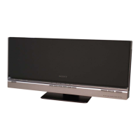
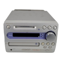
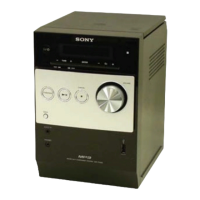
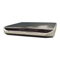
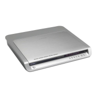
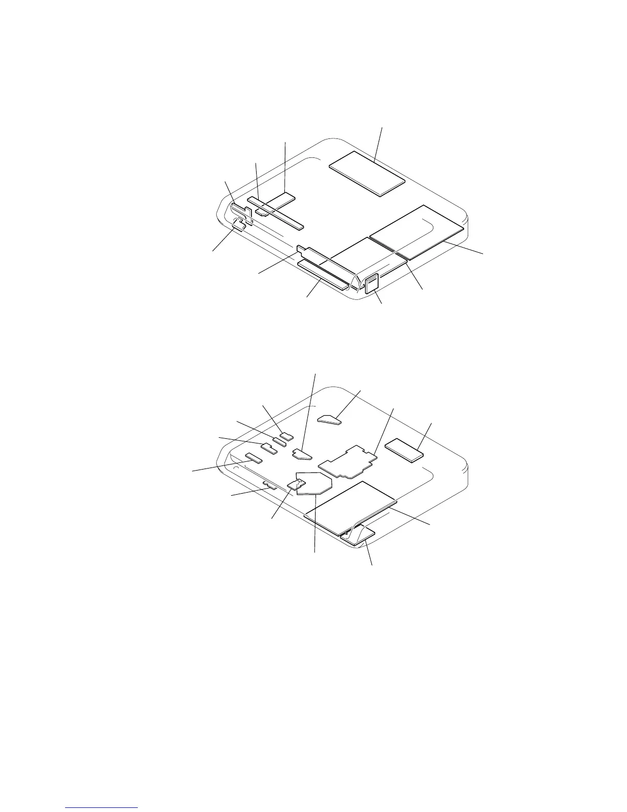
Identifies controls and connectors on the front panel.

Rear Panel Layout

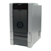
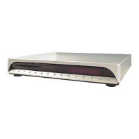
Identifies connectors and jacks on the rear panel.

DIAGRAMS

Circuit Board Locations

Illustrates the physical placement of various circuit boards.

RF Board (Printed Wiring & Schematic)

Physical layout and circuit diagram for the RF board.

DMB08 Board (Printed Wiring & Schematic)

Physical layout and circuit diagrams for the DMB08 board.

AMP Board (Printed Wiring & Schematic)

Physical layout and circuit diagrams for the AMP board.

IO Board (Printed Wiring & Schematic)

Physical layout and circuit diagrams for the IO board.

EXPLODED VIEWS

Case Section Exploded View

Exploded view of the case section with part numbers.

Front Panel Section Exploded View

Exploded view of the front panel section with part numbers.

Mechanism Deck Sections Exploded Views

Exploded views of the mechanism deck sections 1-6.

ELECTRICAL PARTS LIST

Amplifier Section Parts

List of electrical components for the amplifier section.

DMB08 Board Parts

List of electrical components for the DMB08 board.

IO Board Parts

List of electrical components for the IO board.

SUPPLEMENT-1: TEST MODE AND ELECTRICAL ADJUSTMENT

SECTION 1 TEST MODE

Accesses various diagnostic and operational test modes.

SECTION 2 ELECTRICAL ADJUSTMENT

Procedures for electrical adjustments and servo calibration.

SUPPLEMENT-2: DISASSEMBLY, ASSEMBLY, BLOCK DIAGRAMS, IC DIAGRAMS & PIN FUNCTIONS

SECTION 1 DISASSEMBLY

Step-by-step procedure for disassembling the set.

IC Block Diagrams

Diagrams illustrating the internal structure of key integrated circuits.

IC Pin Function Description

Detailed description of each pin's function for key ICs.

SUPPLEMENT-3: TACTILE SWITCH REPLACEMENT NOTES

Servicing Notes on Tactile Switches

Information on selecting tactile switches based on board suffixes.

Tactile Switch Part Number Reference

Table correlating board suffixes with specific tactile switch part numbers.

Related product manuals