Do you have a question about the Sony HCD-FX900W and is the answer not in the manual?
Details output power and total harmonic distortion for various speaker configurations.
Lists video output and input specifications including HDMI and component.
Specifies the voltage and frequency for operation.
Provides approximate physical dimensions of the unit.
Describes AC leakage testing procedure and limits.
Explains how to lock and unlock the disc tray for anti-theft demonstrations.
Safety instruction for discharging capacitors using a specific resistor.
Precautions for installing new optical pick-up units and handling solder bridges.
Instruction on applying adhesive agent when replacing front panel buttons.
Visual guide showing the service position of the MAIN board (Side A).
Visual guide showing the service position of the MAIN board (Side B).
Visual guide illustrating the service position of the DMB12 board.
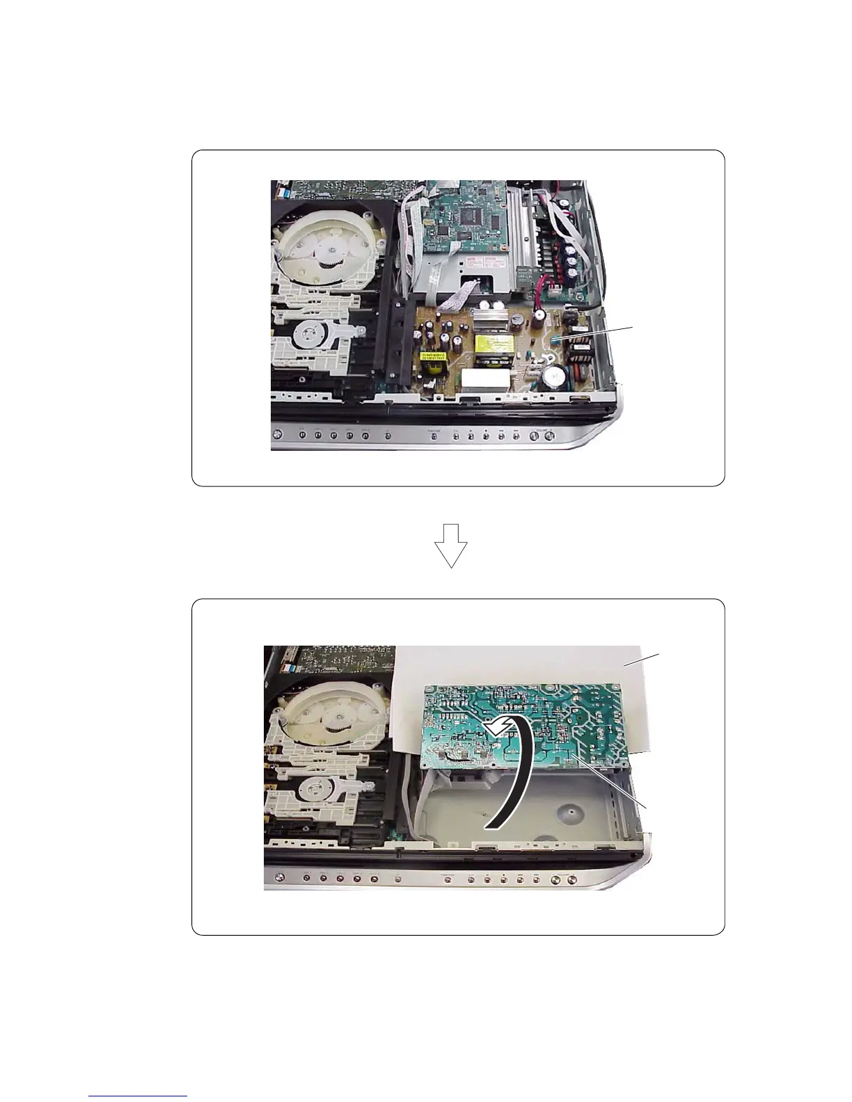
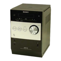
Visual guide showing the service position of the POWER board.
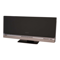
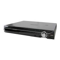
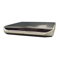
Identifies controls and connectors on the front panel of the unit.
Identifies ports and connectors on the rear panel of the unit.
Explains the meaning of various indicators on the front panel display.
Lists the functions of various buttons on the remote control.
Outlines the step-by-step procedure for disassembling the unit.
Instructions for installing the cam (eject lock) mechanism.
Procedure for installing the cam (gear) component.
Clears all RAM data, resetting the system to initial conditions.
Mode for checking software version, FL, LED, and KEY status.
Function to lock the disc tray for anti-theft demonstration.
Mode used for returning the set to the customer after repair.
Overview of the IOP measurement function for diagnosis and adjustment.
Procedure to enter the Test Mode menu for diagnosis.
Standard procedures for executing IOP measurement.
Resets laser hour data for both CD and DVD.
Resets all emergency history error codes.
Procedures for adjustment and measurement when replacing the base unit.
Adjustment procedure for DIAT signal RF level.
Illustrates the physical location of various circuit boards within the unit.
Waveform for DVDRFIP signal at IC101.
Waveform for XTALI signal at IC101.
Waveform for YUV4 signal at IC101.
Waveform for XIN(I) signal at IC702.
Waveform for CLKIN signal at IC2.
Waveform for Xin signal at IC501.
Waveform for XFSOIN signal at IC3010.
IC block diagram for the RELAY board components.
IC block diagram for DMB12 board components.
IC block diagrams for CXD9883M components on the MAIN board.
Logic diagram for IC671, a SN74LV126APWR IC.
Logic diagram for IC704, a SN74LVC257APWR IC.
Block diagrams for IC3010, IC3020, IC3030, CXD9876R.
Exploded view illustrating the assembly of the main unit components.
Refers to button replacement precautions on page 7.
General notes regarding part number differences and availability.
Instruction on how to reference parts in the list.