79
HCD-FX900W
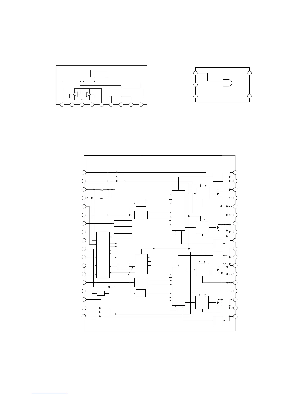
• IC Block Diagrams
IC701, 711, 721 BA6956AN
IC150, IC705 SN74LVC1G08DCKR
– RELAY Board – – DMB12 Board –
1 2 3 4 5 6 7 8 9
CONTROL LOGIC
TSD
VREF
OUT-
OUT+
GND
VCC
VM
IN+
GND
IN-
1
2
3
Vcc
5
GND
4
A
B
Y
– MAIN Board –
IC3100, IC3150, IC3200, IC3250, IC3300, IC3400, IC3500 CXD9883M
1
10
9
8
11
12
13
14
7
6
15
16
17
18
3
4
5
20
19
2
AGND
GND
GND
PGND
PGND
PGND
PGND
PGND
PGND
36
35
34
33
32
31
30
29
28
27
26
25
24
23
22
21
Stuck
Detect
Stuck
Detect
Timing
Control
Timing
Control
Protection
Logic
Protection
Logic
Gate
Drive
Gate
Drive
Gate
Drive
Gate
Drive
Over
Current
Fault
Over
Current
Fault
Over
Current
Fault
Over
Current
Fault
Programmable
Current
sense
OUT_B
OUT_B
OUT_B
PVDD_B
PVDD_B
PVDD_B
OUT_A
OUT_A
OUT_A
PVDD_A
PVDD_A
PVDD_A
REG
BST_B
GVDD_B
VDD
PWM_B
M1
M2
M3
VREG
OC_ADJ
PWM_A
/RESET
/SD
/OTW
GVDD_A
BST_A
Protection
and
Reset
Logic
OLP
OTP
CB3C
Temperature
waming/error
Power-Up
Reset
Under
Voltage
Protection
/HIZ_HS_B
/HIZ_HS_A
/HIZ_LS_B
/HIZ_LS_A
/OCL_B
/OCL_A
/OCH_B
/OCH_A
/RESET_A
/RESET_B
VREG
/HIZ_HS_X
/HIZ_LS_X
/OCH_X
/OCL_X
/RESET_X
/PCR
/UVP
/UVP
/UVP_VREG
VREG
GVDD_A
GVDD_B
VREG
 Loading...