2424
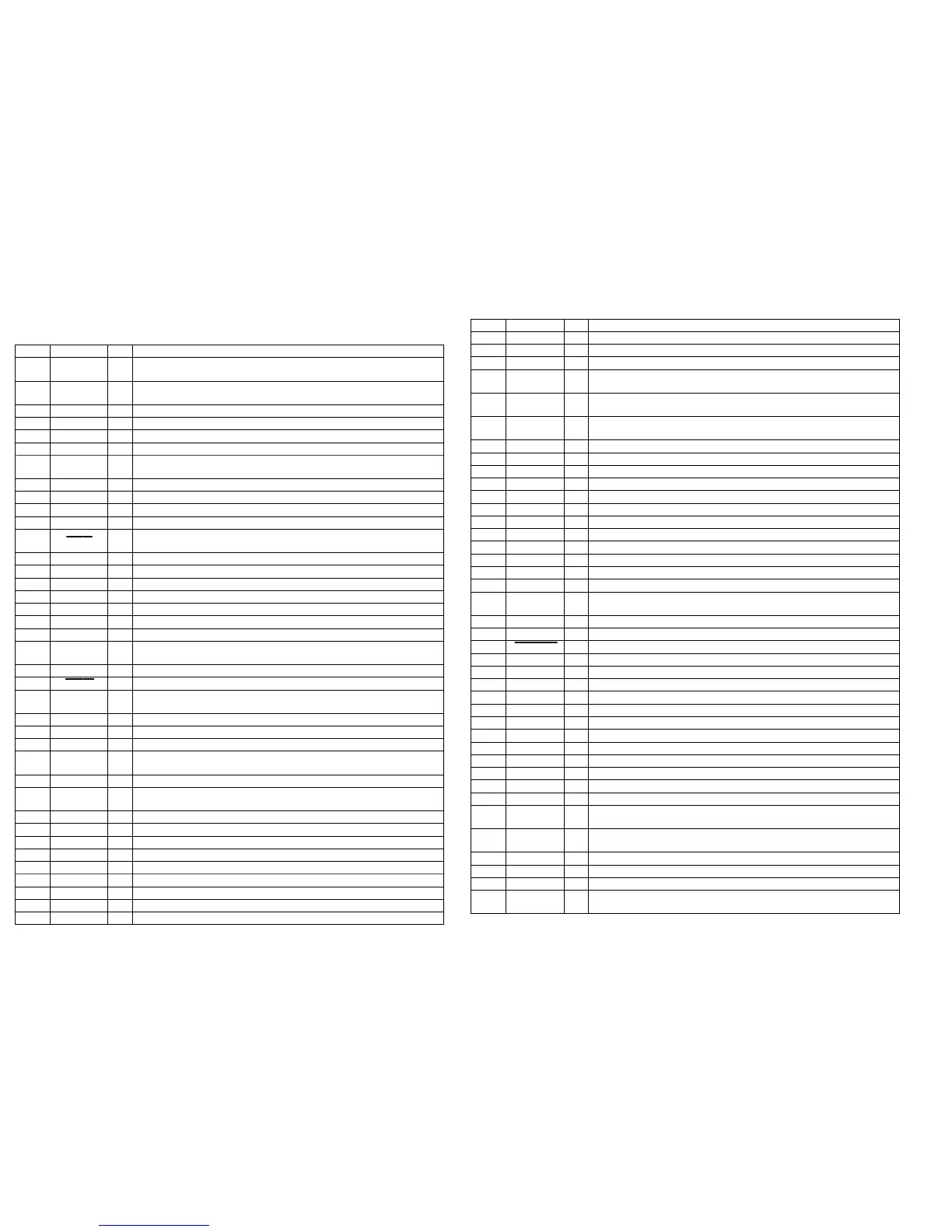
5-14. IC PIN FUNCTION DESCRIPTION
Pin No. Pin Name I/O
Description
39 CLOCK OUT O
Output terminal for the clock signal check Not used (open)
40 VC L+R/L–R O
Virtual cinema L+R/L–R selection signal output terminal Not used (open)
41 XHOLD I
Not used (fixed at “L”)
42 LCD SW O
Liquid crystal display on/off selection signal output terminal “L”: on, “H”: off
Not used (open)
43 STBY RELAY O
Main power on/off control signal output terminal “L”: standby mode, “H”: power on
(Used for the US, Canadian, AEP and UK models only)
44 BASS FREQ O
Sync bass frequency normal/high selection signal output to the M62493FP (IC101)
“L”: sync bass off (normal), “H”: sync bass high Not used (open)
45 OPT SEL O
Not used (open)
46 XWR I
Not used (fixed at “H”)
47 493 DATA O
Serial data output to the M62493FP (IC101)
48 493 CLK O
Serial data transfer clock signal output to the M62493FP (IC101)
49 ST MUTE O
Tuner muting control signal output to the tuner pack “H”: muting on
50 STEREO I
FM stereo detection signal input from the tuner pack “L”: stereo
51 TUNED I
Tuning detection signal input from the tuner pack “L”: tuned
52 ST CE O
PLL chip enable signal output to the tuner pack
53 ST DOUT O
PLL serial data output to the tuner pack
54 ST DIN I
PLL serial data input from the tuner pack
55 ST CLK O
PLL serial data transfer clock signal output to the tuner pack
56 VC BYPASS O
Virtual cinema bypass control signal output terminal Not used (open)
57
PHONES
DETECT
I
Connection detect signal input of the headphone jack (J701)
“L”: no connected, “H”: headphone connected
58 LCD LAT O
Serial data latch pulse output to the liquid crystal display unit (LCD601)
59 LCD A0 O
Address signal output to the liquid crystal display unit (LCD601)
60 LCD RESET O
Reset signal output to the liquid crystal display unit (LCD601) “L”: reset
61 NC O
Not used (open)
62 VCC —
Power supply terminal (+5V)
63 NC O
Not used (open)
64 VSS —
Ground terminal
65 to 68 NC O
Not used (open)
69 JOG B I
Jog dial pulse input from the rotary encoder (S652 JOG) (B phase input)
70 JOG A I
Jog dial pulse input from the rotary encoder (S652 JOG) (A phase input)
71 VOL B I
Jog dial pulse input from the rotary encoder (S651 VOLUME) (B phase input)
72 VOL A I
Jog dial pulse input from the rotary encoder (S651 VOLUME) (A phase input)
73 to 78 NC O
Not used (open)
79 LED FUNCTION O
LED drive signal output of the key illumination indicator (D643 to D648) “H”: LED on
80 LED POWER O
LED drive signal output of the I/1 indicator (D638) “H”: LED on
81 LED TIMER O
LED drive signal output of the TIMER indicator (D637) “H”: LED on
(Used for the US, Canadian, AEP and UK models only)
82 LED LCD O
LED drive signal output of the liquid crystal display back light indicator (D639 to D642)
“H”: LED on
83 LED ENTER O
LED drive signal output of the ENTER indicator (D636) “H”: LED on
84 LED JOG O
LED drive signal output terminal Not used (open)
85 LED CINEMA O
LED drive signal output terminal Not used (open)
86 LED DOLBY O
LED drive signal output of the PRO LOGIC indicator (D633) “H”: LED on
(Used for the STR-NX3 only)
• MAIN BOARD IC501 M30622MA-A12FP (SYSTEM CONTROLLER )
Pin No. Pin Name I/O
Description
1 L+R I
Spectrum analyzer drive signal input from the spectrum analyzer band-pass filter (IC401)
(for VACS, non-stop signal)
2 BPF SL I
Spectrum analyzer drive (super low frequency) signal input from the spectrum analyzer band-pass
filter (IC401) (for 40 Hz)
3 F RELAY O
Speaker protect relay drive signal output for the front side speaker “H”: relay on
4 R RELAY O
Speaker protect relay drive signal output for the rear side speaker “H”: relay on
5 SIRCS I
Remote control signal input from the remote control receiver (IC601)
6 LINE MUTE O
Line muting on/off control signal output terminal “L”: muting on
7 DBFB O
DBFB normal/high selection signal output to the M62493FP (IC101)
“L”: DBFB high, “H”: DBFB low/off
8 BYTE I
External data bus line byte selection signal input terminal Fixed at “L” in this set
9 CNVSS —
Ground terminal
10 XCIN I
Sub system clock input terminal (32.768 kHz)
11 XCOUT O
Sub system clock output terminal (32.768 kHz)
12 RESET I
System reset signal input from the reset signal generator (IC502) “L”: reset
For several hundreds msec. after the power supply rises, “L” is input, then it changes to “H”
13 XOUT O
Main system clock output terminal (16 MHz)
14 VSS —
Ground terminal
15 XIN I
Main system clock input terminal (16 MHz)
16 VCC —
Power supply terminal (+5V)
17 NMI I
Non-maskable interrupt input terminal Fixed at “H” in this set
18 WAKE UP O
Wakeup control signal output to the CPU on the HTC-NX1 “H” active
19 PHONES MUTE O
Muting on/off control signal output terminal “L”: muting on Not used (open)
20 RDS INT I
RDS serial data transfer clock signal input from the tuner pack
(Used for the AEP and UK models only)
21 RDS DATA I
RDS serial data input from the tuner pack (Used for the AEP and UK models only)
22 AC CUT I
AC off detection signal input from the reset signal generator (IC502) “L”: AC cut checked
23 PL CLK O
Serial data transfer clock signal output to the M62464FP (IC201)
(Used for the STR-NX3 only)
24 PL DATA O
Serial data output to the M62464FP (IC201) (Used for the STR-NX3 only)
25 PL LAT O
Serial data latch pulse output to the M62464FP (IC201) (Used for the STR-NX3 only)
26 STK POWER O
Power amplifier on/off selection signal output terminal “L”: standby mode, “H”: on
27
SPEAKER
PROTECT
I
Protect on/off detection signal input from the speaker protect circuit
“L”: protect on, “H”: protect off
28 SOFT-TEST O
Output terminal for the software test Not used (open)
29 IIC CLK I/O
Communication data reading clock signal input or transfer clock signal output with the CPU on
the HTC-NX1
30 IIC DATA I/O
Communication data bus with the CPU on the HTC-NX1
31 TXD1 O
Not used (open)
32 RXD1 I
Not used (fixed at “L”)
33 CLK1 I
Not used (fixed at “L”)
34 RTS1 O
Not used (open)
35 LCD DATA O
Serial data output to the liquid crystal display unit (LCD601)
36 RXD0 I
Not used (fixed at “L”)
37 LCD CLK O
Serial data transfer clock signal output to the liquid crystal display unit (LCD601)
38 493 LT O
Serial data latch pulse output to the M62493FP (IC101)
 Loading...