Hardware layout and configuration UM2324
16/43 UM2324 Rev 4
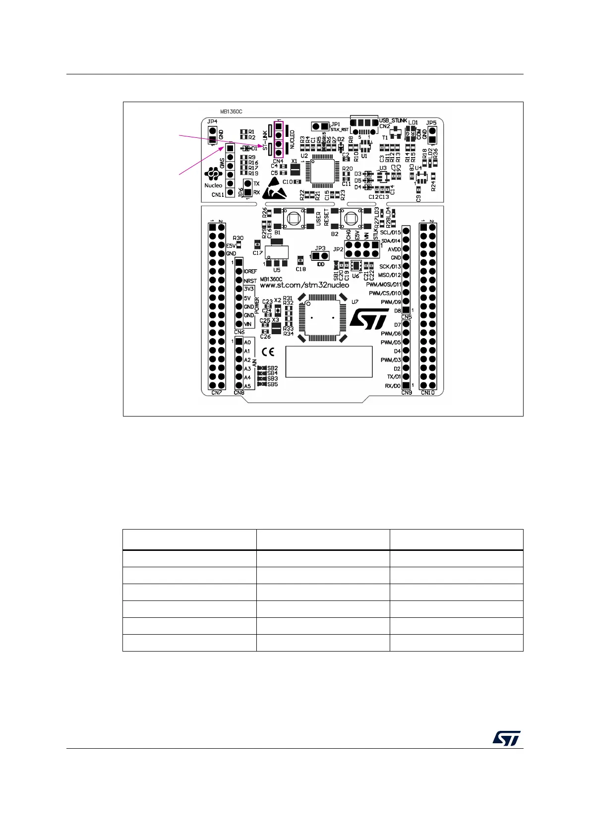
Figure 7. STM32 Nucleo-64 board connections image
6.4.4 Using ST-LINK/V2-1 to program/debug an external STM32 application
It is easy to use the ST-LINK/V2-1 to program the STM32 on an external application.
Remove the 2 jumpers from CN4 as shown in
Figure 8, and connect the application to the
CN11 debug connector according to Table 6.
Note: SB19 must be OFF if CN11 pin 5 is used in the external application.
MSv48501V1
CN4
jumpers ON
CN11
SWD connector
Table 6. CN11 debug connector (SWD)
Pin CN11 Designation
1 VDD_TARGET VDD from the application
2 SWCLK SWD clock
3 GND Ground
4 SWDIO SWD data input/output
5 NRST RESET of target MCU
6SWOReserved
 Loading...