UM2324 Rev 4 19/43
UM2324 Hardware layout and configuration
42
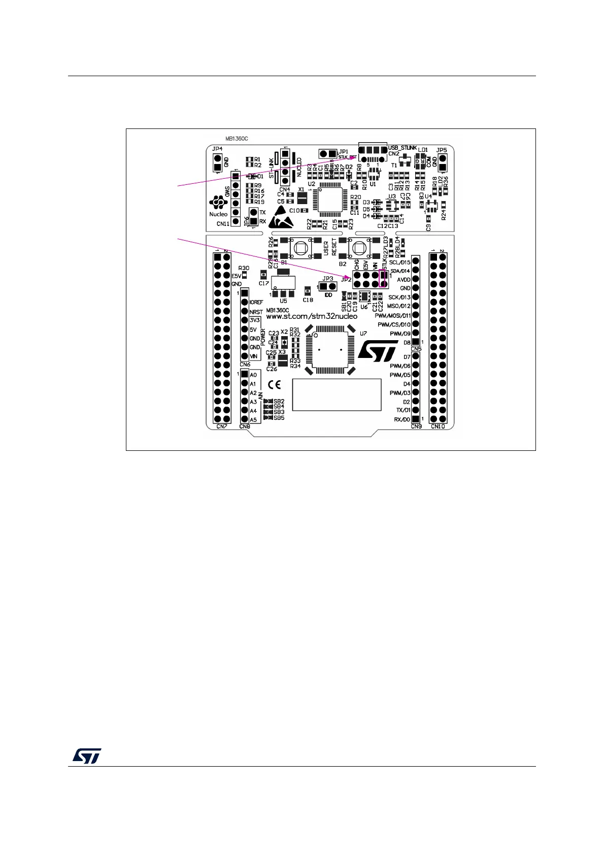
USB power: STLK configuration: the JP2 jumper must be connected as shown in Figure 9.
Figure 9. STLK power source
VIN is the 7 V to 12 V DC power from CN6 pin 8 named VIN on ARDUINO
®
connector
silkscreen or from pin 24 of CN7 ST morpho connector. In this case, the JP2 jumper must be
on pins 3 and 4 to select the VIN power source on the JP2 silkscreen. In that case, the DC
power comes from the power supply through the ARDUINO
®
Uno V3 battery shield
(compatible with Adafruit PowerBoost 500 shield).
MSv48503V1
CN2
USB_STLINK
JP2
PIN 1/2 ON
 Loading...