Theory
of
Operation—
DM
501A
to tin:'
Analog Converter
(U1601
pin
15).
In
ac
current
'll.
the inA ac
front^panel switch
(Sl-L pin
4)
is
closed.
The
voltage developed across the input current
stinfil
OS coupled to AC Buffer
U1539,
which
is
connected
(!"/
Rei;"/
K
'. 528 enenji'er) as a
X10
gain amplifier. The
vollaye at ['in
6 of
U1539 feed through
'11537
to converter
U!s29
(pin
!)
anrl outputs
Ei!
pin
8
of
U1429. Through
apf
irop:
iate sv;itcfiing,
U 1429
pin 8 output voltage couples
to
the
Analog
Converter, U1601 pin 15. Ac current is also
rneas'i'cd as a true rms ac function.
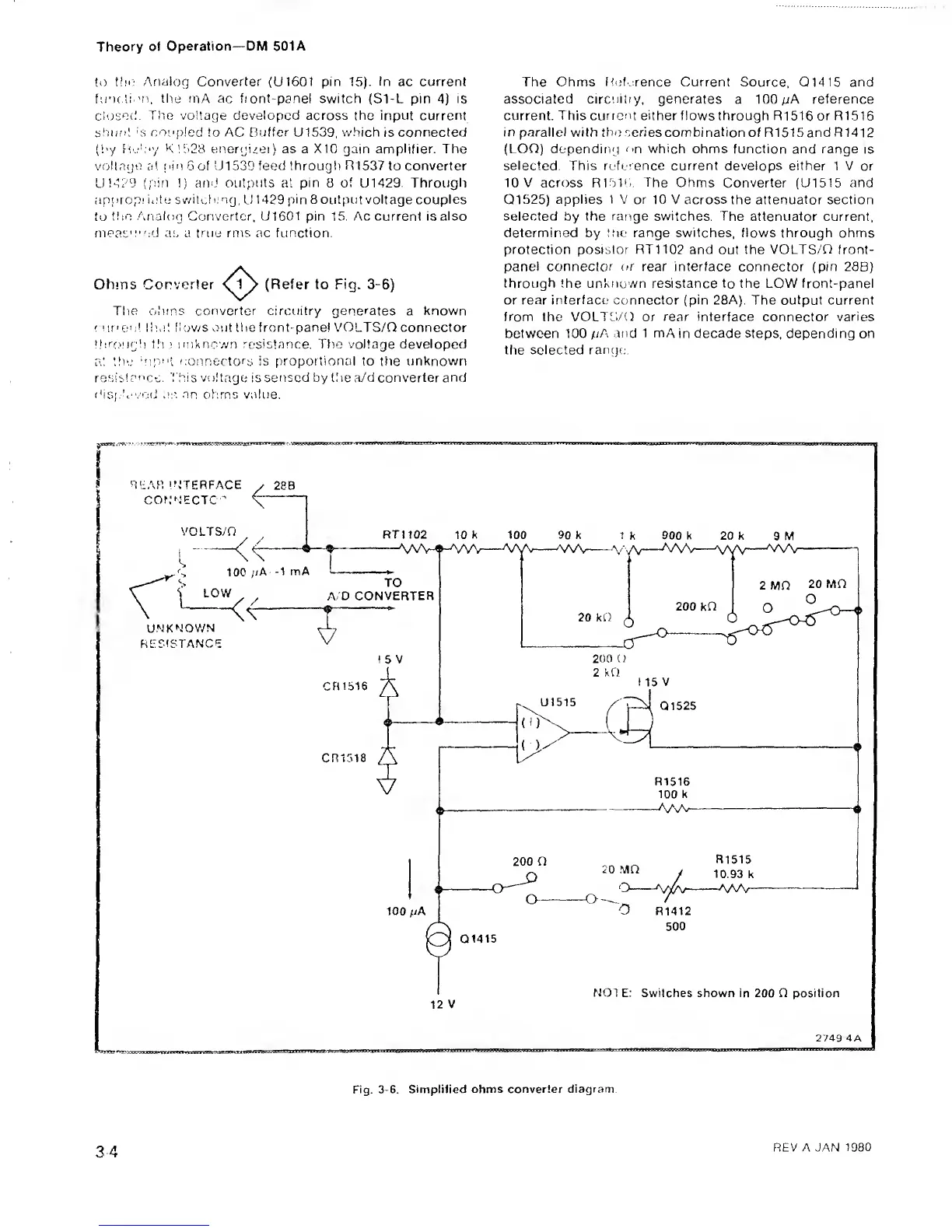
Ohms Cortverter (Refer to Fig. 3-6)
Tlie ohms converter circuitry generates
a
known
(
1
ir'C'
1.
I hat Mov/s out
II
le front-pane!
VOLTS/Q
connector
Ihrourh
t,'!
,'
unknown resistance. ITie voltage
developed
at
tile
''ipi'i
connectors is proportional to tfie unknown
resislc'ce.
This voltage
is sensed by
Uioa/d
converter
and
('is,c'c-'.''ed us an
ottrns
value.
The Ohms
Rirfurence
Current Source, Q1415 and
associated circuitry, generates
a
100
pA
reference
current.
This current either
flows through R1516 or R1516
in parallel with the series combination
ofR1515andRl412
(LOO)
depending
on
which ohms function and range
is
selected. This reference current develops either
1 V or
10 V across
Rthli-.
The Ohms
Converter (U1515
and
Q1525)
applies
1
V or 10
V
across
the attenuator
section
selected
by
the
range
switches. The
attenuator current,
determined by
the
range
switches,
flows through ohms
protection
posislor RT1102
and out the
VOLTS/0
front-
panel connector
or
rear interface connector (pin
28B)
through the unknown resistance
to
the LOW front-panel
or
rear
interface
connector
(pin
28A). The output current
from the
VOLTB/O
or
rear interface
connector
varies
between
100 .and 1 mA in decade steps,
depending
on
the selected
range
2749 4A
Fig.
3-6.
Simplified
ohms converter
diagram
 Loading...