With
the
jumper in
the
dBm
mode, R1535 (dB0) is
adjusted for
0
dBm when the
0
dB range
switch is
depressed and
0.7746 Vac
is
connected between
the
VOLTS/O and LOW
front-panel connectors.
When the
jumper is
in
the dBV
mode
and
the
input
signal
is 1.000 Vac, the display readout is
also
0
dB. The
signal
at U1429
(pin
7)
is
internally
buffered
and
applied to
pin
6
(dB BUF
OUT). This signal
changes approximately
“3
mV
per 1 dB
change.
The positive
temperature coef-
ficient resistor (RT1525)
is used to provide
compensation
for the
0.3%
per degree
C
temperature
drift in the dB
converter
of
U1429.
Potentiometer R1528 (dB Gain)
in combination with
U1538 (dB
AMP), RT1525, and
feedback resistor R
1536,
is
used to scale the dB buffer
output
signal
to 100 mV perdB
at the input of
U1538
(pin
6).
This
output signal feeds
through switch sections
S3 and SI, to resistor R1613
(located
on diagram
2),
then into the Analog
Converter
(U1601 pin
15).
When dB is
selected, the
display is limited to 0.1 dB
resolution.
This reduced
resolution occurs
when dB
switch S3-A
(pin
3)
connects
15
V to
ni::it Select
Diiver
U1701
(pin
1).
The output
of UI701 (,"in
IG)
iurns
on
diodes CR1605
and CR1607,
disabling ti;3
digit
seiect
lines for the two least
significant
digits in die
display
(DS1200 and
DS1101). Simuitrir:eoL:Sg',
i 5
\'
is
coupU-n
through diode CR1711
turning on the
.SIGN fidSIOOO)
in
the
display, liiis same
tiigh Livel
disables mtegratod
circuits
UI703A, U1703B,
and
U17C5B
c
.
l
o.iaLlPs
U1705A.
The
decimal point
is di- play^J
un.:uiiu
most signifinant digit langes.
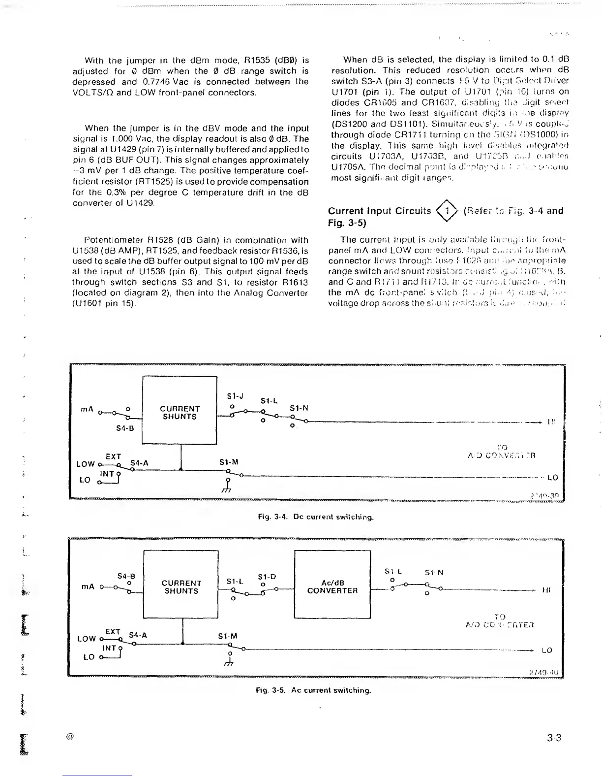
Current
Input Circuits (Refer
'.c
rig
3-4
and
Fig. 3-5)
^
The current input
i.s only available
Ihicugli tiic fior.t-
panel mA and
LOW
con:
eclors. Input
to the
niA
connector
flows through
luso
f 1C26
oiui
iin
.ipprof.iiate
range switch and
shunt resist jrs roiisis'i
g
.-<i
liiGf'ui,
B.
and C and
RI
71 I and R1710. I; o'c
.luiro.ii, .'unclio.
.
"'itn
the
mA
dc front-panel s vilch
(t .
.J
pin
4)
c.os
'd,
i
.i-
voltage drop
across
the .si.
uni
n-sistor.s
ii
d.ie
,1:
Fig.
3-4.
Dc
current switching.
Fig.
3-5.
Ac
current switching.
 Loading...