1
1
2
2
3
3
4
4
5
5
6
6
D D
C C
B B
A A
3 4
P ower Path Supplies
6/19/2 015
HVL117D_Power_Path.Sch Doc
Sheet Title:
S ize:
Mod. Date:
Fi le:
Sheet: of
B
http://www.ti.co m
Con tact:
j-ontiveros@ ti.co m
TPS65982EVMProje ct Title:
Des igned for:Pu blic Release
Assembly Va riant: -001
© Tex as Instrument s 2015
Drawn By:
Engineer:
Jacob Ontiveros
Te xas I nstruments an d/or its li censors do not wa rrant the accuracy or co mpleten ess of this sp ecifi cation or an y inform ation conta ined therein. Te xas Instruments and/or its li censors do not
warrant that this design wi ll meet the specificati ons, w ill be suitable fo r yo ur a pplicati on or fit for any particular purpose , or will operate in an i mplementation. Te x as I nstruments an d/or its
licensors do no t warra nt that the de sign is pro duction worth y. You shoul d complete ly validate and t est your d esign im ple mentation to c onfir m the system functionality f or your application.
Not in version c ontrolSVN Rev:
HVL117Number: R ev: D
VIN
1
VSE NSE
6
EN
8
RT
10
G ND
3
COMP
7
P H
2
B OOT
9
P AD
11
G ND
4
GND
5
U5
TPS54335D RCR
0.1µF
C26
0.1µF
C20
100k
R82
0.1µF
C23
DNP
C27
DNP
DNP
C30
DNP
DNP
R81
DNP
DNP
R83
DNP
G ND
GND
GND
GND
GND
GND
0.1µF
C37
0.1µF
C31
100k
R92
19.1k
R94
0.1µF
C34
DNP
C38
DNP
DNP
C41
DNP
DNP
R93
DNP
G ND
GND
GND
GND
GND
GND
0.1µF
C48
0.1µF
C42
100k
R102
0.1µF
C45
DNP
C49
DNP
DNP
C52
DNP
DNP
R101
DNP
DNP
R103
DNP
G ND
GND
GND
GND
GND
GND
22µF
C46
22µF
C47
G ND
VIN
1
VSE NSE
6
EN
8
RT
10
G ND
3
COMP
7
P H
2
B OOT
9
P AD
11
G ND
4
GND
5
U6
TPS54335D RCR
G ND
VIN
1
VSE NSE
6
EN
8
RT
10
G ND
3
COMP
7
P H
2
B OOT
9
P AD
11
G ND
4
GND
5
U7
TPS54335D RCR
G ND
22µF
C35
22µF
C36
22µF
C24
22µF
C25
S yste m _3V 3
S yste m _5V
HV _Source
1
2
3
J5
DNP
32.4k
R84
7.1 5k
R104
S ENS E
1
GND
4
P OWE R
2
P OWE R
3
GND
5
S HIELD
6
SHIELD
7
SHIELD
8
SHIELD
9
J4
JPD1135 -509-7 F
E xt erna l Po wer
G ND
TP5
S3
1.00k
R27
Sys tem _RE S ET
Tiva_5VS yste m _5V
Tiva_3V 3S yste m _3V 3
1 2
3 4
J7
DNP
10µF
C33
10µF
C22
10µF
C44
DNP
R91
DNP
J9
47.5k
R97
47.5k
R109
8.45k
R95
100pF
C39
2200pF
C40
9.53k
R108
91pF
C50
1800pF
C51
330pF
C28
5600pF
C29
2.74k
R85
47.5k
R88
Sys te m_3V 3
Sys te m_5V
Ext ernal Power
External Power
External Power
S ys tem _3V3
HV_S ourc e
12V _V SENSE
12V_VSENSE
5V _V SENS E
5V_VSENSE
3V 3_VS EN S E
3V3_VSENSE
G ND
10uH
L4
10uH
L3
10uH
L2
Schematic
www.ti.com
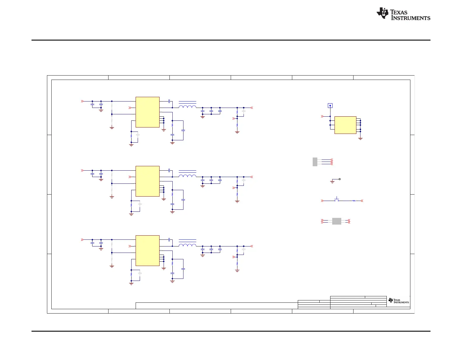
The circuit diagram in Figure 4 shows the schematic for page 2 of the TPS65982-EVM. Page 2 includes power path-related ICs: the
External_Power to System_3V3 buck converter (U5) and passive components, the External_Power to System_5V buck converter (U6) and passive
components, the External_Power to HV_Source buck converter (U7) and passive components, the Barrel Jack receptacle (J4), the power rail
header (J5), the Tiva to System power jumper (J7), and the System_RESET push-button (S3).
Figure 4. TPS65982-EVM Schematic Page 2
30
TPS65982 Evaluation Module SLVUAF8C–June 2015–Revised November 2015
Submit Documentation Feedback
Copyright © 2015, Texas Instruments Incorporated

 Loading...