A
1
2
3
4
5
6
7
8
9
10
BCDEFGH I JK
L MN
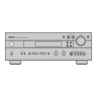
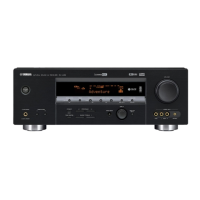
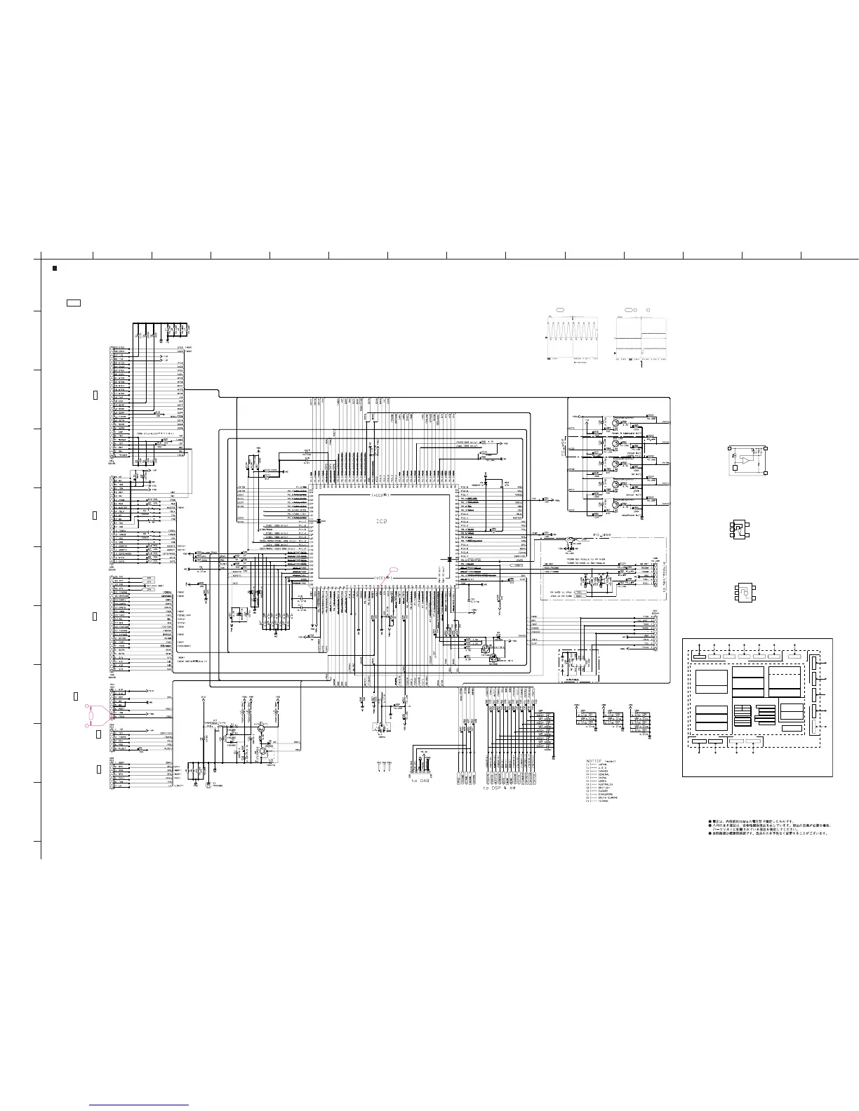
RX-V459/HTR-5940/HTR-5935/DSP-AX459
SCHEMATIC DIAGRAMS
69
★ All voltages are measured with a 10MΩ/V DC electronic volt meter.
★ Components having special characteristics are marked s and must be replaced
with parts having specifications equal to those originally installed.
★ Schematic diagram is subject to change without notice.
DSP 1/3
5.0
-11.9
4.9
5.0
5.0
4.3
5.0
-11.9
4.9
5.0
-11.9
4.9
5.0
5.0
4.3
00.2
5.0
0
5.0
0.1
0
1.2
3.3
0.1
0
0.2
5.0
5.0
5.0
5.0
5.0
0.1
0.1
0.1
10.1
0
5.8
5.8
5.8
5.2
5.2 5.2
5.0 5.0
5.0
4.3
0.1
0.1
4.9
0
5.1
4.9
5.0
5.0
0.40
2.70
2.00
2 1
B-2
5.0
0.1
0
0
0
0
0
0
0
0
0
0
0
0
0
2.7
2.0
0.4
5.0
1.0
5.2
5.2
0
4.3
5.2
4.9
4.9
4.9
4.9
4.8
0.5
0.6
0.1
4.9
0
0
5.0
5.0
5.0
4.9
2.5
0
2.4
5.0
5.0
5.0
0
5.0
5.0
5.0
5.0
5.0
0
0
5.0
5.0
5.0
5.0
5.0
5.0
5.0
0.1
5.0
0
5.0
5.2
4.9
4.9
4.9
0
0
0
0
0
0
0
5.0
4.9
4.9
4.9
4.9
0.1
0.1
0.1
0.1
4.9
5.0
0
0
5.0
0
0.1
4.9
0
0
0
0
0.1
4.8
5.0
5.0
5.0
4.9
0.1
5.0
5.0
4.9
4.9
0
0
5.9
0
4.9
4.9
0
0
0
5.0
0.1
0
0
0
0
0
0
A-1
to FUNCTION (1)_CB200
Page 72
C2
to OPERATION (1)_CB309
Page 73
C9
to FUNCTION (2)_CB291
Page 72
I3
to MAIN (1)_W1026
Page 74
H2
to OPERATION (4)_W3009
Page 73
XX
to MAIN (1)_W1007
Page 74
H1
to FLASH WRITER
DSP
MICRO PROCESSOR
2
1
3
Vref
V
OUT
GND
V
IN
–
+
IC1 : RH5RE58AA-T1-FA
Voltage regulator
Y4
B2
GND 3
IC4, 5 : SN74AHCT1G32DCKR
Single 2-input positive-OR gate
Vcc5A1
Y4
B2
GND 3
IC6 : SN74AHC1G08DCKR
2-input positive-AND gate
IC2 : M30625MHP-A98GP
2-input positive-AND gate
Vcc5A1
8
(3) (3) (3) (3)
8882
Por t P0
Port P11 Port P14 Port P12
<VCC2 ports> (4)<VCC1 ports> (4)
NOTES:
1. ROM size depends on microcomputer type.
2. RAM size depends on microcomputer type.
3. Ports P11 to P14 exist only in 128-pin version.
4. Use M16C/62PT on VCC1=VCC2.
Watchdog timer
(15 bits)
Watchdog timer
(
Polynomial: X
16
+X
12
+X
5
+1
)
Clock synchronous serial I/O
(8 bit x 2 channels)
Watchdog timer
(15 bits)
XIN-XOUT
XCIN-XCOUT
PLL frequency synthesizer
On-chip oscillator
Three-phase motor
control circuit
Timer (16 bit)
Output (timer A): 5
Input (timer B): 6
Internal peripheral functions
M16C/60 series 16-bit CPU core Memory
Multiplier
ROM
(1)
RAM
(2)
R0H R0L
R1H
R2
R3
A0
SB
USP
ISP
INTB
PC
FLG
A1
FB
R1L
DMAC
(2 channels)
D/A converter
(8 bit x 2 channels)
D/A converter
(
10 bit x 8 channels
Expandable up to 26 channels
)
UART or
clock synchronous serial I/O
(8 bit x 8 channels)
Por t P1 3
Port P1 Port P2 Port P3 Port P4 Port P5 Port P6
Port P7 Port P8 Port P8_5 Port P9 Port P10
88888 8
87 88
<VCC2 ports> (4) <VCC1 ports> (4)
<VCC1 ports> (4)
POINT A-1 Pin 18 of IC2 POINT B-2 1 / Pin7, 2 / Pin8 of CB3
POWER ON
(connect the power cable)
M30625MHP-A98GP
 Loading...