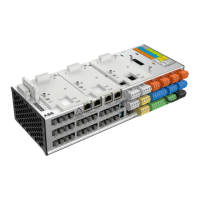
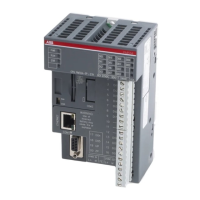
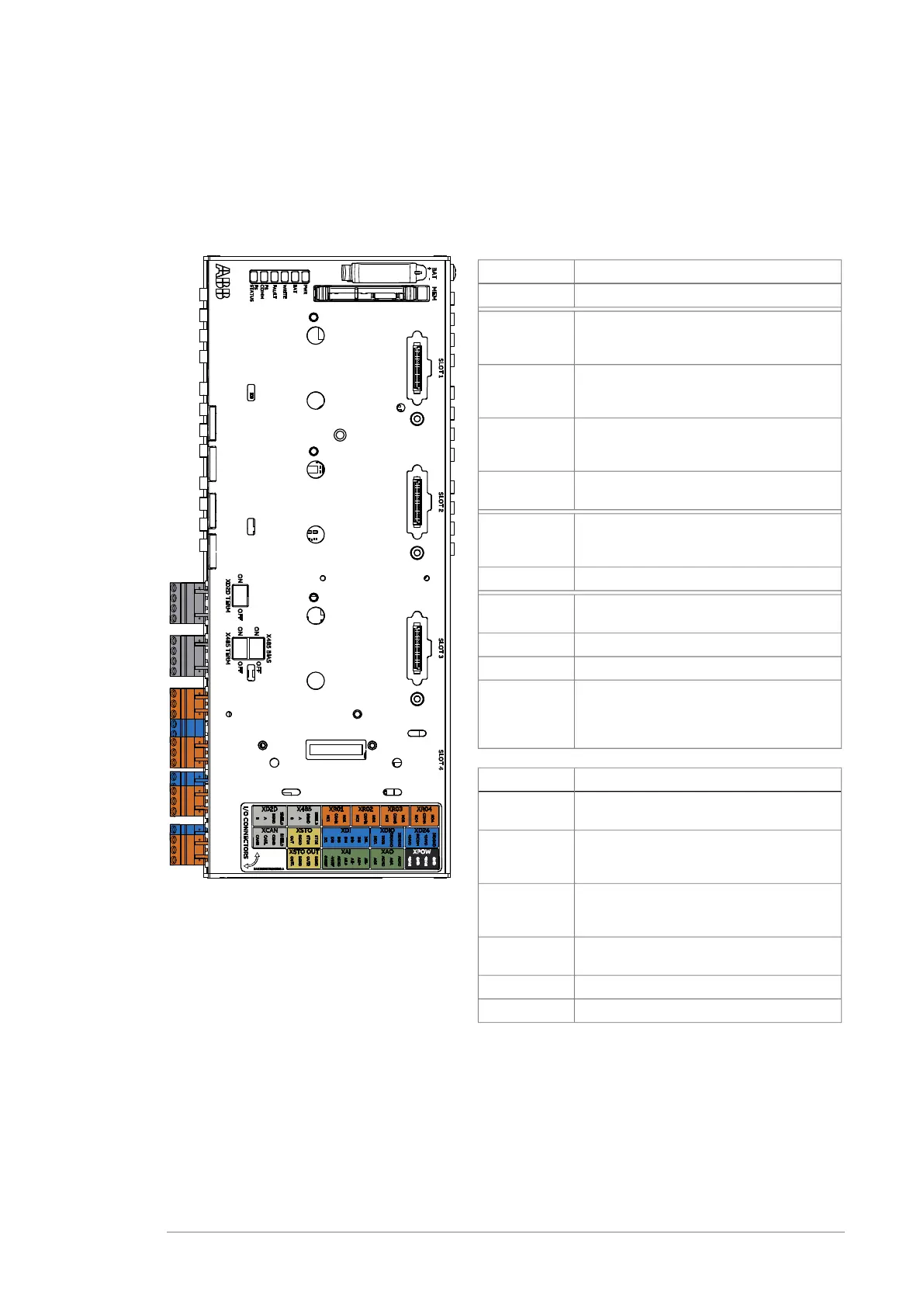
Layout
The figures show the layout of the control unit.
For the default I/O connection diagrams and more information on the connections,
refer to the applicable hardware manual.
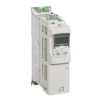
Description
I/O terminalsI/O
I/O extension, encoder interface or fieldbus
adapter module connection. For F-type
modules with USCA-02 adapter.
SLOT 1
I/O extension, encoder interface or fieldbus
adapter module connection. For F-type
modules with USCA-02 adapter.
SLOT 2
I/O extension, encoder interface or fieldbus
adapter module connection. For F-type
modules with USCA-02 adapter.
SLOT 3
RDCO-0x DDCS communication option
module connection
SLOT 4
UMU-01 memory unit connection. Data logger
microSDHC memory card for inverter module
communication is inside the memory unit.
MEM
Holder for real-time clock battery (BR2032)BAT
Termination switches for drive-to-drive link
(XD2D)
XD2D TERM
RS-485 link termination switchX485 TERM
RS-485 link bias switch.X485 BIAS
Ground selection. Determines whether DICOM
is separated from DIOGND (ie. the common
reference for the digital inputs floats). Refer
to the ground isolation diagram.
DICOM=
DIOGND
DescriptionLED
When the PWR LED is on, the voltage supply
is sufficient.
PWR
When the BAT LED is on, the real-time clock
battery voltage is higher than 2.5 V. If the LED
is off, replace the battery.
BAT
When the WRITE LED is on, writing to
microSDHC memory card is in progress. Do
not remove the microSDHC memory card.
WRITE
The control program has generated a fault.
Refer to the firmware manual.
FAULT
Reserved.FS COMM
Reserved.FS STATUS
Operation principle and hardware description 11
 Loading...