80
Test Point Locations
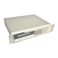
Figure 6-2 is a foldout diagram that illustrates the location of 45 test points on the main circuit board. The test points are
described in Table 3-3 and are used in various troubleshooting procedures provided in Chapter 3.
Component Location Diagram
Figure 6-2 is a foldout diagram that will aid you in locating electrical components on the main board assembly. The diagram
is divided into a numerical matrix of columns and rows. Table 5-4 gives the part number and description of each electrical
part .
Table 6-1. Schematic Diagram Notes
1. All resistors are in ohms ±1%, 1/8 W, unless otherwise specified.
2. All capacitors are in microfarads unless otherwise specified.
3. All unmarked capacitors are 0.047µF.
4. An asterisk negates a signal name. For example, CS2 appears on the schematic as CS2*.
5. Signal lines that are terminated by flags continue on other sheets (see Table 6-2). Note that flags do not indicate
signal flow direction.
—————————— SPCLR*
6. Unterminated signal lines simply go to another location of the same schematic sheet (see Table 6-3). The following is
an example of such a signal.
—————————— TRIG
7. Values of resistors and capacitors that are enclosed by a heavy rectangle □ apply to model 6060B only. Refer to the
parts list for the model 6063B values.
 Loading...