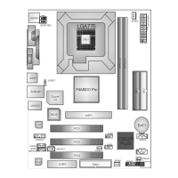
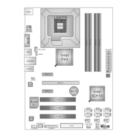
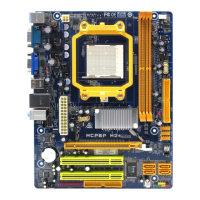
P35D2-A7
36
CAS Latency Time
When synchronous DRAM is installed, the number of clock cycles of CAS
latency depends on the DRAM timing.
The Choices: Auto (default), 5, 6.
DRAM RAS# to CAS# Delay
This field allows you to insert a timing delay between the CAS and RAS strobe
signals, used when DRAM is written to, read from, or refreshed. Low value
will provide a faster performance; and high value made the system more stable.
This field applies only when synchronous DRAM is installed in the system.
The Choices: Auto (default), 5, 6.
DRAM RAS# Precharge
If an insufficient number of cycles are allowed for RAS to accumulate its
charge before DRAM refresh, the refresh may be incomplete, and the DRAM
may fail to retain data. Low value will provide faster performance; and high
value made the system more stable. This field applies only when synchronous
DRAM is insta lled in the system.
The Choices: Auto (default), 5, 6.
Precharge dealy (tRAS)
T his item allows you to specify the minimum row active time (tRAS).
The Choices: Auto (default),9, 10,11,12,13,14,15,16,17,18,19,20,21,22,23,24.
TWR
The Choices: Auto (default),3,4,5,6,7,8,9, 10,11,12,13,14,15.
TWTR
The Choices: Auto (default),2,3,4,5,6,7,8,9, 10,11,12,13,14,15.
TRRD
The Choices: Auto (default),2,3,4,5,6,7,8,9, 10,11,12,13,14,15.
TR TP
The Choices: Auto (default),2,3,4,5,6,7,8,9, 10,11,12,13,14,15.
CPU Voltage
This item allows you to select CPU Voltage Control.
The Choices: StartUp (default), +0.012V ~ +0.787V.
FSB Termination Voltage
This item allows you to select FSB termination Voltage.
The Choices: 1.25V (d efault), 1.35V, 1. 45V, 1.55V.
 Loading...