- 8 -
6.CIRCUIT EXPLANATION
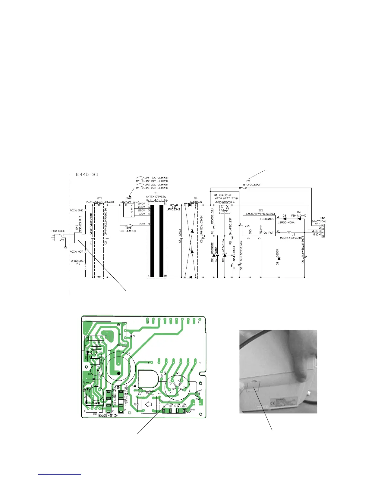
6-1. Power supply circuit
The power supply circuit provides the following voltage for the main circuit.
Output Pin No1----- VC1 (DC32.3V): To the VC line for the VFD Display power. (Not used for CE-6000)
Output Pin No.2---- VC2 (DC24V): To the Vp line for the printer power.
Output Pin No.3---- VLED (DC5.85V): To the Vcc,Vcc2 and Vdd for the logic circuit power.
Output Pin No.4---- GND: Signal GND.
The power switch SW1 is located at the right side of the lowercase.
After connected the power plug into AC outlet and turn on the SW1, the transformer T1 will
genarate the about AC33V to secondary side. Then, after rectifier circut, the VC1 (DC32.3V)
is supplied to the VC line for display power (for the drive of display tube. Not for LED model.)
The IC2 is the shunt regulator for the control of Q1 transistor. This circuit is genarate the
VC2 (DC24V) for the printer power. The IC1 is regulator for 5V power supply.
Power supply PCB E445-S1
Voltage selector
(Not used for CE-6000)
Power SW1 cover
Power switch SW1
Note: F3 is not used for
CE-6000.
NOTE: Voltage selector is not used for CE-6000.
 Loading...