— 15 —
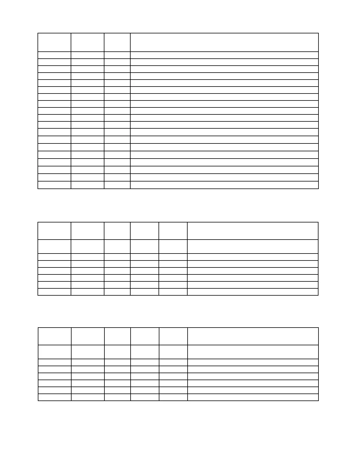
Pin No. Name In/Out Description
46 RA20 Out Not used
47 R15 Out Address bus
48 VSS(GND) In GND terminal
49 VH3(VCC) In 9V input
50 VL3 In 6V input
51 CAC Out Address bus
52 MS7 Out Address bus
53 MSO Out Chip enable signal for ROM (Not used)
54 MS4 Out Chip select signal for RAM (Not used)
55 MS1 Out Chip select signal
56 MS5 Out Not used
57 MS2 Out Not used
58 MS6 Out Chip select signal
59 BZ1 Out Buzzer signal
60 OTP In Connected to GND
61 BZ2 Out Buzzer signal
62 SWO Out Main switch control signal
63 VH4(VCC) In 9V input
64 TXO Out Transmission data output terminal
Operation program ROM pin descriptions
RAM pin descriptions
Pin No. Name In/Out Status Status Description
of OFF of ON
3~12, 23 A0~A15 In L Pulse Address bus line (A0~A15)
25~28, 31
13~15, 17~21 IO0~IO7 Out L Pulse Data bus line (IO0~IO7)
16 GND In L L GND terminal
22 S1 In H Pulse Chip enable signal from Gate array
24 OE In L Pulse Output enable signal from Gate array
29 W In H Pulse Write enable signal from CPU
32 VCC In L H VDD terminal
Pin No. Name In/Out Status Status Description
of OFF of ON
2~12,23, A0~A17 In L Pulse Address bus line (A0~A14, RA15~RA17)
25~30
13~15, 17~21 O0~O7 Out L Pulse Data bus line (IO0~IO7)
16 GND In L L GND terminal
22 CE In H Pulse Chip enable signal from Gate array
24 OE In L Pulse Output enable signal from Gate array
31 A18 In L Pulse Address line (RA18)
1, 32 VPP, VCC In L H VDD terminal
 Loading...