Schematic Diagrams
B - 1
B.Schematic Diagrams
Appendix B: Schematic Diagrams
Table B - 1
SCHEMATIC
DIAGRAMS
This appendix has circuit diagrams of the W950BU / W955BU notebook’s PCB’s. The following table indicates where
to find the appropriate schematic diagram.
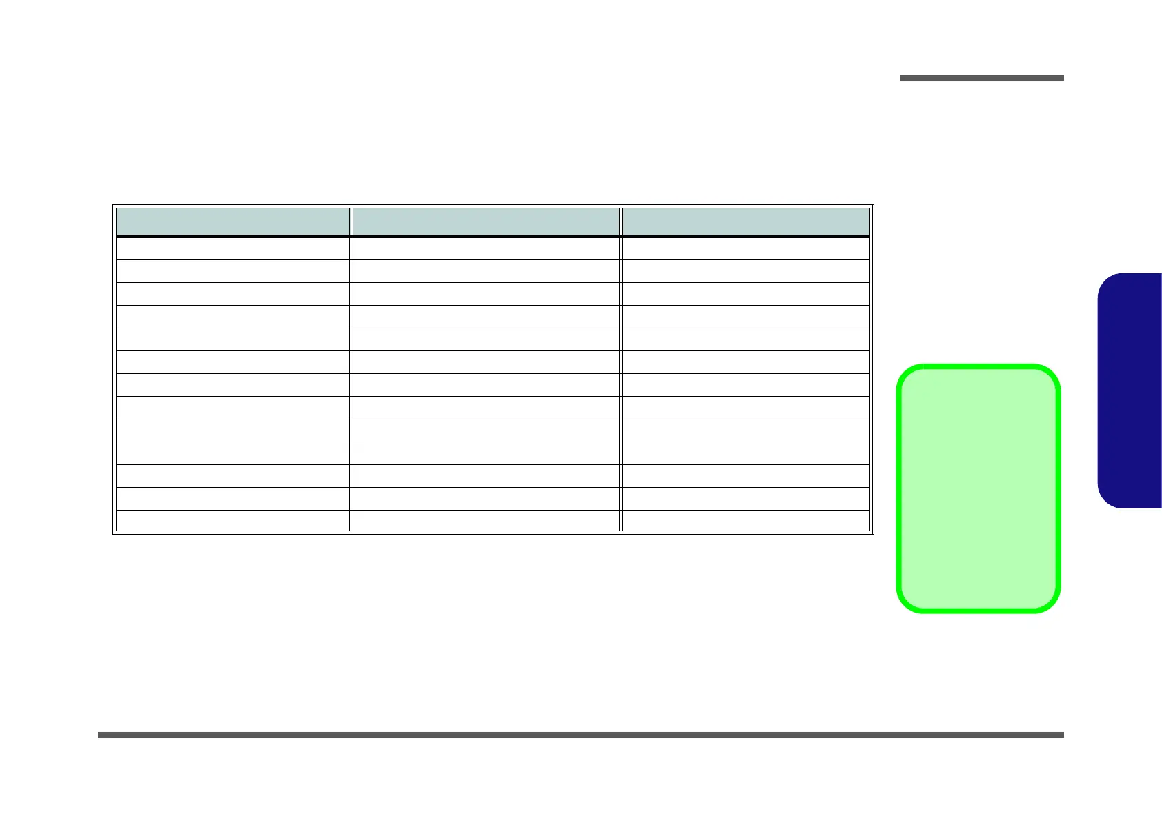
Diagram - Page Diagram - Page Diagram - Page
System Block Diagram - Page B - 2 DDR3L SO-DIMM_B_0 - Page B - 15 VDD3, VDD5 - Page B - 28
Skylake ULT - Page B - 3 Panel, Inverter - Page B - 16 VDDQ, VDDQ_VTT, 1.5VS, 1.8VS - Page B - 29
Skylake ULT DDR - Page B - 4 CRT - Page B - 17 1.0V Series - Page B - 30
Skylake ULT RTC/HDA/CLK/SD - Page B - 5 PS8625 - Page B - 18 VCore, VCCGT, VCCSA, VCCIO - Page B - 31
Skylake ULT LPC/SPI/SMB - Page B - 6 Card Reader & RTL8411B - Page B - 19 Charger, DC-In - Page B - 32
Skylake ULT Power Maint - Page B - 7 HDMI, RJ45, Fan - Page B - 20 NCP81206 Regulator - Page B - 33
Skylake ULT GPIOS/I2C/EMMC - Page B - 8 M.2 (WLAN, 3G, SSD) - Page B - 21 Audio Board - Page B - 34
Skylake ULT PCIE, USB, SATA - Page B - 9 Audio Codec - Page B - 22 Power SW Board - Page B - 35
Skylake ULT Power 1 - Page B - 10 USB 3.0, G Sensor, TPM - Page B - 23 Option BOM List - Page B - 36
Skylake ULT Power 2 - Page B - 11 KBC ITE IT8587 - Page B - 24 ODD to HDD Board - Page B - 37
Power-VSS - Page B - 12 CCD, MIC, LID, I/O Connector - Page B - 25 External ODD Board - Page B - 38
CFG, RSVD, VCCGT - Page B - 13 HDD, ODD, LED - Page B - 26 Battery Con. Board - Page B - 39
DDR3L SO-DIMM_A_0 - Page B - 14 3V, 5V, 3VS, 5VS - Page B - 27 LID Switch Board - Page B - 40
Version Note
The schematic dia-
grams in this chapter
are based upon ver-
sion 6-7P-W95J4-003.
If your mainboard (or
other boards) are a lat-
er version, please
check with the Service
Center for updated di-
agrams (if required).
 Loading...