60
AVR-2808CI / AVR-988
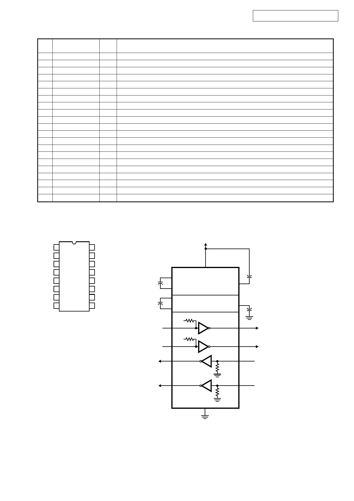
HIN202EIBNZ-T (MC:IC104)
Function
Pin
No.
Pin Name I/O
* For latch-up countermeasure, perform each power supply ON/OFF in the same timing.
28 XOUT O X tal osc. connecting output terminal
29 XIN I X tal osc. connection, external clock input terminal (24.576MHz or 12.288MHz)
30 DVDD „ Digital power
31 DGND „ Digital GND
32 EMPHA/UO I/O Emphasis information/U-data output/Chip address setting terminal
33 AUDIO/VO I/O Non-PCM detect/V-flag output/ Chip address setting terminal
34 CKST I/O Clock switch transition period output/Demodulation master or slave function switching terminal
35 INT I/O Interrupt output for ∝com (Interrupt factor selectable)/Modulation or general I/O switching terminal
36 RERR O PLL lock error, data error flag output
37 DO O ∝com I/F, read out data output terminal (3-state)
38 DI I ∝com I/F, write data input terminal
39 CE I ∝com I/F, chip enable input terminal
40 CL I ∝com I/F, clock input terminal
41 XMODE I System reset input terminal
42 DGND „ Digital GND
43 DVDD „ Digital power
44 TMCK/PIO0 I/O 256fs system clock input for modulation/General I/O in/output terminal
45 TBCK/PIO1 I/O 64fs bit clock input for modulation/General I/O in/output terminal
46 TLRCK/PIO2 I/O fs clock input for modulation/General I/O in/output terminal
47 TDATA/PIO3 I/O Serial audio data input for modulation/General I/O in/output terminal
48 TXO/PIOEN O/I Modulation data output/ General I/O enable input terminal
14
15
16
9
13
12
11
10
1
2
3
4
5
7
6
8
C1+
V+
C1-
C2+
C2-
R2
IN
T2
OUT
V
CC
T1
OUT
R1
IN
R1
OUT
T1
IN
T2
IN
R2
OUT
GND
V-
V
CC
+5V
2
V+
16
T1
OUT
T2
OUT
T1
IN
T2
IN
T1
T2
11
10
14
7
+5V
400k
+5V
400k
R1
OUT
R1
IN
R1
1312
5k
R2
OUT
R2
IN
R2
89
5k
+10V TO -10V
VOLT AGE INVERTER
0.1 F
6
V-
C2+
C2-
+
0.1 F
4
5
+5V TO 10V
VOLT AGE INVERTER
C1+
C1-
+
0.1 F
1
3
+
0.1 F
+
GND
 Loading...