4 - 1
SECTION 4 CIRCUIT DESCRIPTION
4-1 RECEIVER CIRCUITS
4-1-1 ANTENNA SWITCHING CIRCUIT
The antenna switching circuit functions as a low-pass filter
while receiving and a resonator circuit while transmitting.
The circuit does not allow transmit signals to enter receiver
circuits.
Received signals enter the antenna connector (J1) and pass
through the low-pass filters (L1–L3, C2, C3, C8–C10). The
filtered signals are passed through the
λ
⁄4 type antenna
switching circuit (D5, D6, L5) and then applied to the RF cir-
cuit.
4-1-2 RF CIRCUIT
The RF circuit amplifies signals within the range of frequen-
cy coverrage and filters out-of-band signals.
The signals from the antenna swiching circuit pass through
the tunable bandpass filter (D7, L8). The filtered signals are
amplified at the RF amplifier (Q1) and then enter the anoth-
er three-stage bandpass filters (D9–D11, L12, L13) to sup-
press unwanted signals. The filtered signals are applied to
the 1st mixer circuit.
D7, D9–D11 employ varactor diodes, that are controlled by
the PLL lock voltage, to track the bandpass filter. These var-
actor diodes tune the center frequency of an RF pass band
for wide bandwidth receiving and good image response
rejection.
4-1-3 1ST MIXER AND IST IF CIRCUITS
The 1st mixer circuit converts the received signal to fixed
frequency of the 1st IF signal with the PLL output frequency.
By changing the PLL frequency, only the desired frequency
will pass through a pair of crystal filters at the next stage of
the 1st mixer.
The RF signals from the bandpass filter are mixed with the
1st LO signals, which come from the Rx VCO circuit via the
buffer amplifier (Q3), at the 1st mixer circuit (Q2) to produce
a 21.75 MHz 1st IF signal. The 1st IF signal is passed
through the matching circuit (L15, L52) and a pair of crystal
filters (FI1) in order to obtain selection capability and to pass
only the desired signals. The filtered signal is applied to the
2nd IF circuit after being amplified at the 1st IF amplifier
(Q4).
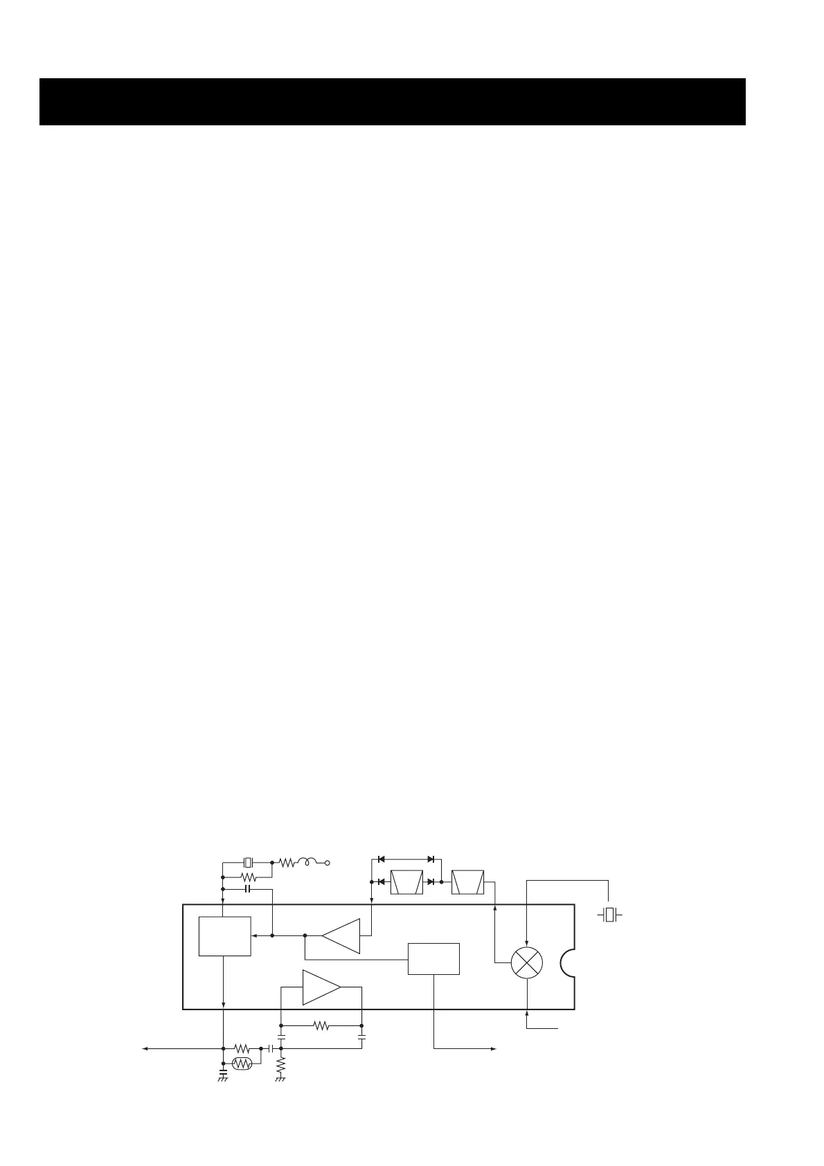
4-1-4 2ND IF AND DEMODULATOR CIRCUITS
The 2nd mixer circuit converts the 1st IF signal into a 2nd IF
signal. The double-conversion superheterodyne system
(which convert receive signals twice) improves the image
rejection ratio and obtains stable receiver gain.
The 1st IF signal from the IF amplifier (Q4) is applied to the
2nd mixer section of the FM IF IC (IC1, pin 16) and is then
mixed with the 2nd LO signal for conversion into 455 kHz
2nd IF signal.
IC1 contains the 2nd mixer, 2nd local oscillator, limiter ampli-
fier, quadrature detector, active filter and noise amplifier cir-
cuit. The local oscillator section and X1 generates the
21.295 MHz 2nd LO signal.
The 2nd IF signal from the 2nd mixer (IC1 pin 3) passes
through the ceramic filters (FI3 and FI4) during narrow chan-
nel spacing selection or passes through FI4 (bypassing FI3)
only during wide channel spacing selection to suppress
unwanted heterodyne frequencies signals via the N/W
switches (D501, D502).
The filtered signal is applied to the quadrature detector sec-
tion in the FM IF IC to demodulate the 2nd IF signal into AF
signals using the ceramic discriminator (X2) after being
amplified at the limiter amplifier section (pin 5). The demod-
ulated AF signals are output from pin 9 of the IC and applied
to the AF circuit via the receiver mute citcuit.
The N/W switches (D501, D502) select a ceramic filter (FI3
or bypass), and the other N/W switch (Q61) adjusts the input
level to the FM IF IC (IC1, pin 8) to switch the bandwidth
depending on the NWC signal from the CPU (IC20, pins 57)
When NWC signal is high, bandwidth setting is wide.
 Loading...