4 - 3
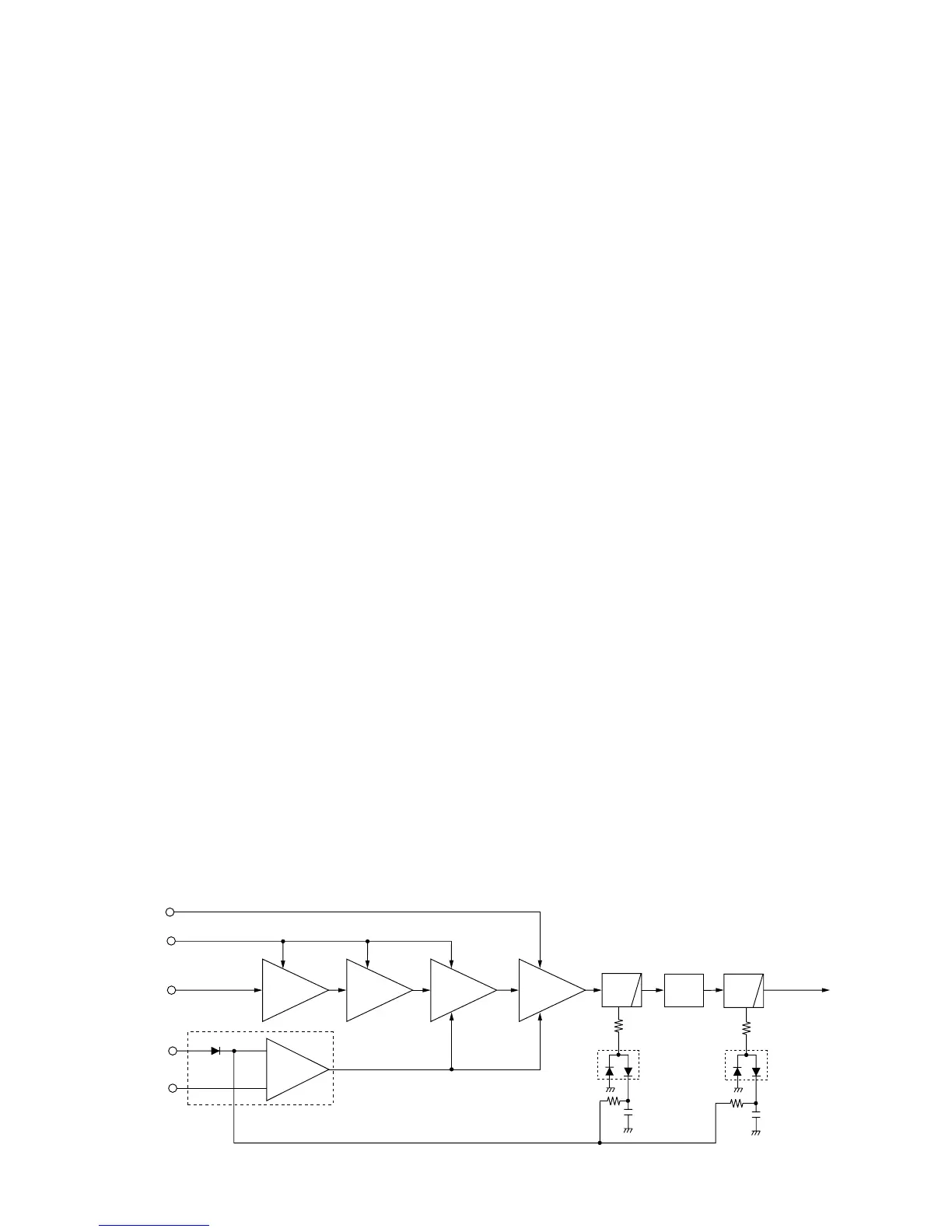
The filtered AF signals are applied to the FM/PM switch
(MAIN unit; IC11, pin 6), and pass through the low-pass fil-
ter (MAIN unit; IC5, pin 1). The amplified signals are applied
to the D/A converter (MAIN unit; IC6, pin 4)
The output signals from the D/A converter (MAIN unit; IC6,
pin 3) are applied to the modulation circuit (MAIN unit; D18).
4-2-2 MODULATION CIRCUIT (MAIN UNIT)
The modulation circuit modulates the VCO oscillating signal
(RF signal) using the microphone audio signals.
The AF signals from the D/A converter (IC6, pin 3) change
the reactance of varactor diode (D18) to modulate the oscil-
lated signal at the TX VCO circuit (Q14, D17). The modulat-
ed VCO signal is amplified at the buffer amplifiers (Q10,
Q11) and is then applied to the drive amplifier circuit via the
T/R switch (D14).
The CTCSS/DTCS signals (“CENC0”, “CENC1”, ”CENC2”
from the CPU (FRONT unit; IC401, pins 79–81) pass
through the low-pass filter (IC403, pins 1, 3), and are then
applied to the D/A converter via the “CDCS” line (IC6, pin 9).
The output signal from the D/A converter (IC6, pin 10) pass-
es through the low-pass filter (IC5, pins 1, 2). The
CTCSS/DTCS signals are mixed with “MOD” signal at the
low-pass filter (IC5), and are then applied to the D/A con-
verter again (IC6, pin 4).
4-2-3 DRIVE/POWER AMPLIFIER CIRCUITS
The drive/power amplifier circuits amplify the VCO oscillat-
ing signal to an output power level.
The signal from the VCO circuit passes through the T/R
switch (D14), and is amplified at the YGR (Q5, Q9), drive
(Q8), power (Q7) amplifiers to obtain 4 W of RF power (at
7.2 V DC).
The amplified signal is passed through the low-pass filter
(L4, C12, C13, C16), power detector (D1, D39), antenna
switching circuit (D2) and other low-pass filter (L1, L2, L45,
C1–C5, C365), and is then applied to the antenna connec-
tor (CHASSIS unit; J1).
The bias current of the drive (Q8) and power (Q7) amplifiers
are controlled by the APC circuit.
4-2-4 APC CIRCUIT (MAIN UNIT)
The APC circuit (IC2, D1, D39) protects the drive and power
amplifiers from excessive current drive, and selects output
power of HIGH, LOW2 or LOW1.
The power detector circuit (D1, D39) detects the transmit
power output level and converts it into DC voltage. The out-
put voltage is at a minimum level when the antenna imped-
ance is matched at 50 Ω and is increased when it is mis-
matched.
The detected voltage is applied to the differential amplifier
(IC2, pin 3), and the “T2” signal from the D/A converter (IC6,
pin 14), controlled by the CPU (FRONT unit; IC401), is
applied to the other input for reference. When antenna
impedance is mismatched, the detected voltage exceeds
the power setting voltage. Then the output voltage of the dif-
ferential amplifier (IC2, pin 4) controls the input current of
the drive (Q8) and power (Q7) amplifiers to reduce the out-
put power.
4-3 PLL CIRCUITS
4-3-1 PLL CIRCUIT (MAIN UNIT)
A PLL circuit provides stable oscillation of the transmit fre-
quency and receive 1st LO frequency. The PLL output com-
pares the phase of the divided VCO frequency to the refer-
ence frequency. The PLL output frequency is controlled by
the divided ratio (N-data) of a programmable divider.
The PLL circuit contains the TX/RX VCO circuits (Q13, Q14,
D16, D17). The oscillated signal is amplified at the buffer
amplifiers (Q11, Q12) and then applied to the PLL IC (IC4,
pin 8) after being passed through the low-pass filter (L32,
C206, C208).
The PLL IC contains a prescaler, programmable counter,
programmable divider and phase detector, etc. The entered
signal is divided at the prescaler and programmable counter
section by the N-data ratio from the CPU. The divided signal
is detected on phase at the phase detector using the refer-
ence frequency.
If the oscillated signal drifts, its phase changes from that of
the reference frequency, causing a lock voltage change to
compensate for the drift in the oscillated frequency.
 Loading...